5

I am building a small amplifier which is working just fine. While experimenting I interchanged the TL072s with NE5532s and the amplifier stopped working, so I set up a simple non-inverting amplifier to check why.

Here is the schematic + circuit:

schematic

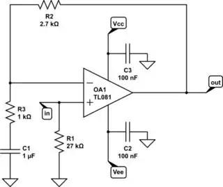
simulate this circuit – Schematic created using CircuitLab

Circuit

Problem: I noticed that the non-inverting input is taking in about 200uA current which is obviously not the max. 800nA input bias current from the data sheet. So with the 27k resistor it's at about -6 to -7 volts, doesn't matter if I connect a signal source or not and the output swings to the negative rail.

My Guess: I know that the NE5532 uses a pair of input protection diodes which I guess are the cause of this current since the circuit works using a TL072. If that is the case: How do I end up forward biasing them? I really want to understand what is happening here. If that is not the case: What am I doing wrong?

Things I tried out / found out:

  1. The circuit works just fine with a TL072
  2. Removing the 1uF capacitor
  3. Using a different NE5532
  4. Lowering the supply voltage of +/-15V symmetrically, I noticed that the voltage drop over the 27k resistor is more or less about quarter of the total supply voltage. (7V for +/-15V)
  5. With the capacitor the output sits at about -14V which makes sense.

I'd really appreciate any help - thanks in advance.

rootsroots
  • 51
  • 4
  • Hi rootsroots, just a tip, you can also draw schematics using the schematic tool (button) just above the text box when editing your question. – JYelton Oct 20 '21 at 15:37
  • Hi! Thank you - I'll try it out. – rootsroots Oct 20 '21 at 15:57
  • Your +/- 15V DC supplies have a common mid-point, which *should* be ground. Does this point connect to the OPamp circuit ground (that is: to the bottom of the 27k resistor, R1)? – glen_geek Oct 20 '21 at 16:28
  • Yes, it's +/-15V from the bottom of the R1 to the power rails. – rootsroots Oct 20 '21 at 16:39
  • What is the purpose of C1? Normally the non-inverting configuration would have the bottom of R3 connect directly to ground. – nsayer Oct 20 '21 at 17:58
  • 1
    To reduce DC gain. It's really just a high pass filter. The absolute value of R3 and C1 in series rises with falling frequency so gain approaches 1 for low frequencies. – rootsroots Oct 20 '21 at 18:36
  • 1
    Are you actually measuring the 200 uA current, or are you inferring it from the voltage? If so, check that your 2.7k is actually good (not open) or perhaps it's not making good contact with the perfboard. Get a different 2.7 k resistor, and this time cut the leads a little longer. And are you measuring your 7 volts on both the op amp pin AND the resistor? If the op amp is not making good contact, that could account for it as well. Never trust that kind of board. The sockets under the plastic shield can break and you won't know it. – WhatRoughBeast May 26 '22 at 13:46
  • Hi. Thanks for your reply. But I don't think this is the problem since the circuit worked perfectly with a TL082! – rootsroots Jun 09 '22 at 15:36

3 Answers3

1

As you guessed, there is a pair of diodes (the block diagram shows them as BJTs with the base connected to the collector, but that’s essentially the same idea) cross-connecting the two inputs. This essentially means that you can’t have more differential voltage than a diode drop or the diodes will conduct and sink current.

I ran into a similar issue and asked here a while ago and the response was that I should add a couple of series resistors on both inputs. This is essentially the simplified schematic on the first page of the datasheet.

That by itself doesn’t explain why an output bias is showing up. For that, I suspect that bias is charging C1. I would try adding a high value resistor across C1 to keep that from happening. C1 can still serve its purpose.

nsayer
  • 1,543
  • 1
  • 18
  • 35
0

The breadboard picture and schematic don't appear to match up. The NE5532 is a dual op-amp. You have R1, R2 and R3 connected to the "A" amplifier, and the yellow wires connected up to the "B" amplifier.

You should ground pins 5 and 6 of the chip and move the yellow wires over to pins 1 and 3. The idea being that you should pin the inputs of the unused amplifier to ground.

nsayer
  • 1,543
  • 1
  • 18
  • 35
  • The amp in the left hand side of the chip matches the schematic. The amp in the right hand side is wired as a voltage follower with its input grounded. – Finbarr Oct 20 '21 at 18:21
  • That's as may be, but it is still not what the schematic shows. – nsayer Oct 21 '21 at 04:04
  • It's exactly the same. The OPA on the right side on the breadboard is not shown in the diagram. – rootsroots Oct 21 '21 at 11:28
  • How is the input getting into pin 3 and the output out from pin 1? – nsayer Oct 22 '21 at 14:06
  • There is no input connected to it. R1 should pull the non inverting input near ground - but it doesn't, that's the problem. The output is loaded by the feedback network. But that doesn't matter because adding a load resistor or a signal source does not make a difference. – rootsroots Oct 22 '21 at 14:52
-2

Remove the 27 k resistor, i.e. directly ground the + input. The resistor is creating a DC offset due to the input current.

  • 2
    Read the data sheet. Worst-case input bias current for an NE5532 is 1 uA. 27k will only develop 27 mV. Given the low AC gain, that's not the problem. – WhatRoughBeast May 26 '22 at 13:38
  • The fact remains that the 27 K is not needed at all (precisely because the input bias current is 1 µA max.) and may be causing harm, such as maybe high-frequency oscillation due to stray capacitance from the output to the + input. – John Woodgate May 27 '22 at 10:44
  • AND - the circuit needs a DC reference voltage in case the input is AC coupled at the source. – AnalogKid Jun 29 '22 at 19:48