3

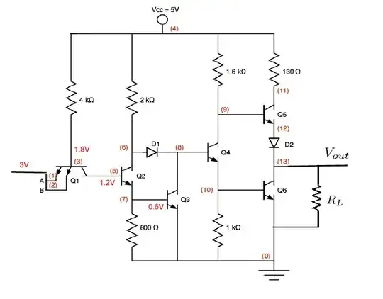
Consider the following logic circuit:

enter image description here

Approach:

Consider the following 2 cases:

  1. Any , or both the inputs are low (0 V): The base of Q1 will be at 0.6 V. A current 1.1 mA flows through the 4K resistor to the base, which saturates Q1. Hence the collector is at 0.2 V. Also, I don't think there will be any collector current, which means Q2 is OFF, which further implies Q3 is also OFF, since Q2 will have no collector current (== Q3 will have no base current).

If Q3 is off, then the current due to the 5V supply flows through the diode D1 into the base of Q4, which means Q4 is ON. Now the collector current from Q4 enters the base of Q6, hence Q6 is also ON.

The emitter of Q6 is at 0 V, hence the base of Q6 is at 0.6 V==emitter of Q4, hence the base of Q4 is at 1.2 V, which means the P side of D1 is at 1.8 V. Also, The collector Q4=== Base of Q5= 0.8 V. If we assume D2 to be forward biased, then this will mean the emitter of Q5 is at 0.8 V, which means Q5 is reverse biased. This suggests that the collector current should be 0 == current through .130K resistor. The simplifications look like this:

enter image description here

Clearly, Vout=0.2 V (LOW), and a current 0.2/RL = 0.01 mA flows through the RL. However, the issue I have with this is , with Q5 OFF, I really cant properly visualise how current can flow through RL. Since with Q5 off, there is no emitter current, so no current through the diode.

Also, I can't seem to properly reason why Q2 will be OFF.

  1. Both the inputs are high (3 V): If we trace back the voltages from Q3, and assume the base-collector junction of Q1 is forward biased we get these voltages:

enter image description here

So the base-emitter junction of Q1 is reverse biased and there is no emitter current, Hence collector current = base current in value, and the collector current flows out of the collector, into the base of Q2 which turns on Q2,which implies Q3 is also ON. Now I am not really sure why, but if we assume Q4 to be OFF, this will imply Q6 is also OFF, and also, Q4 being OFF implies the base of Q5 is pulled high so Q5 is ON.

enter image description here

This is the final situation. Considering Q5, the currents can be written as: \$I_{c} = 5 - (Vo + 0.8)/.130\$ mA, \$I_{b} = 5 - (Vo + 1.2)/1.6\$ mA, \$I_{e} = Vo/R_{l}=Vo/20\$ mA. Using Ie= Ib+Ic, we can solve for Vo, and we get \$Vo=4.145 V\$, i,e HIGH. So it seems that this circuit is behaving as an AND gate, and we have more or less calculated all the currents, now that we know Vo.

My final questions:

  1. Why is Q2 OFF in case 1?

  2. Given Q5 is OFF, how from where exactly can we expect a current flow of 0.01 mA through RL in case 1?

  3. Can the collector current (Q1 of case 2) really flow out of the collector?

  4. Why is Q4 OFF in case 2?

satan 29
  • 189
  • 5
  • Try to read these answers: First https://electronics.stackexchange.com/questions/396680/totem-pole-bipolar-circuit-explanation/396739#396739 the second one https://electronics.stackexchange.com/questions/368455/why-is-d2-switched-off-and-t4-not-in-saturation-mode-in-7408-ttl-gate-as-shown-b/368467#368467 and maybe this one https://electronics.stackexchange.com/questions/304642/ttl-nand-gate-totem-pole-current-and-voltage-analysis/304722#304722 Do you still have some issues? – G36 Sep 07 '21 at 12:23
  • Try considering that Q1 is not a "transistor" but simply 3 diodes (common point of diodes (on base Q1) are anodes. 2 cathodes are inputs A and B (it is ok), last diode between base of Q1 and cathode on base of Q2. This is a "DTL logic". – Antonio51 Sep 07 '21 at 15:57
  • See the last picture of answer from @G36 – Antonio51 Sep 07 '21 at 16:08

1 Answers1

3

Why is Q2 OFF in case 1?

What bothers you exactly about \$Q_2\$ OFF state? Notice that the \$Q_2\$ base voltage will be well below \$0.6V\$ due to \$Q_1\$ saturation.

Given Q5 is OFF, how from where exactly can we expect a current flow of 0.01 mA through RL in case1?

Yes, \$Q_5\$ will be Cut-OFF. \$D_2\$ diode job is to ensure that \$Q_5\$ will be cut-off.

schematic

simulate this circuit – Schematic created using CircuitLab

Notice that to "open" the \$Q_5\$ we need to have:

$$V_{CE4(sat)} + V_{BC6} > V_{BE5} + V_{D2}$$.

And \$V_{BC6} = V_{b6} - V_{C6} = 0.6V - 0.2V = 0.4V\$

Therefore

$$V_{CE4(sat)} + V_{BC6} > V_{BE5} + V_{D2}$$.

$$0.2V + 0.4V > 0.6V + 0.6V$$.

$$0.6V > 1.2V $$

Which is not the case. Therefore \$Q_5\$ will be cut-off due to the presence of diode \$D_2\$, simply there will not be enough voltage across \$Q_5\$ base-emitter junction to turn it on, so \$Q_5\$ will be cut-off.

So, \$Q_5\$ cut-off and \$Q_6\$ is saturated. And in saturation transistor's base-emitter junction is forward biased and the collector-base junction is also forward biased. And because \$R_L\$ resistor is pulling the \$Q_6\$ collector to GND. The forward biased collector-base junction current will flow into \$R_L\$ through this resistor to GND.

schematic

simulate this circuit

Can the collector current (Q1 of case 2) really flow out of the collector?

Notice that \$Q_1\$ is an NPN transistor and his emitter is connected to Vcc. The base is also pull-up to Vcc via a 4k resistor. Therefore the base-emitter junction is reversed biased. So in a normal situation \$Q_1\$ should be will cut-off. But in this case, we have \$Q_1\$ collector is connected directly to \$Q_2\$ base. And this changes the situation completely. There is a path for a \$Q_1\$ base current from Vcc to GND. The \$Q_1\$ base current can flow from:

Vcc--->4k--->Q1 Base-collector junction ---->Q2 Base-emitter junction--->GND.

Notice that the \$Q_1\$ base-collector junction is now forward biased, and the is why the current can flow. So in this scenario, \$Q_1\$ is working in inverse mode also known as a reverse active region.

Also, keep in mind that

schematic

simulate this circuit

Why is Q4 OFF in case 2?

Why? Simply because \$Q_4\$ base voltage is below 0.6V.

Why do you think that \$Q_4\$ is not cut-off?

G36
  • 13,642
  • 1
  • 18
  • 33