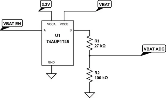
You might find an inverter you can use instead of D1A. You would be looking for an inverter that has very low quiescent current, can tolerate 3.8 V at its VCC power rail, and will still recognize 3.3V cmos input levels when powered from 3.8V.
For example TI p/n SN74AUP1T04DCKR is close. The only problem is that 3.8 V is outside the recommended operating conditions for VCC (but still far from the absolute maximum...).
I also found this one: Nexperia p/n 74AHC1G04GV,125.
It looks like it would recognize your 3.3 V cmos input levels even when it is powered from 3.8 V. Quiescent current and input leakage current could become a bit of a concern. The quiescent current is given as 1uA maximum at 25 C, but it goes up quite a bit with temperature. Not sure if your circuit will be exposed to high temperatures.
The other option is to keep your existing structure with two FET's, but eliminate R4 and R5 (which shouldn't be needed if you drive the gate of D1A with 3.3 V gpio). And then set R6 to a much higher value such as 1 Mohm or even 10 Mohm. If you go to 10 Mohm you will have to make sure that the leakage current in D1A does not cause D1B to turn on unexpectedly. This problem will be most likely to manifest at higher temperatures when the FET's get kind of leaky.
Keep in mind that R6 only conducts current when D1B is on. If the load switched by D1B is at least 100 uA or more, then maybe you can just use 1 MOhm for R6 and not worry too much about the extra 3.8 uA. On the other hand, if the load switched is very small, then I can see how the extra 3.8 uA could be a concern.

