5

I'm working on a class AB amplifier that is used to either source or sink current. The reason for using MOSFETs is space constaints and that high power BJTs are only available in large leaded packages.

I tried to look around for some biasing circuits to reduce crossover distortion, but most designs use BJTs. The main problem I'm seeing with biasing a MOSFET class AB stage is the change in \$V_\mathrm{gs,th}\$ with temperature and within manufacturing tolerances like 2V to 4V. So a simplified design example like this does not appear to be effective given a range of threshold voltages:

schematic

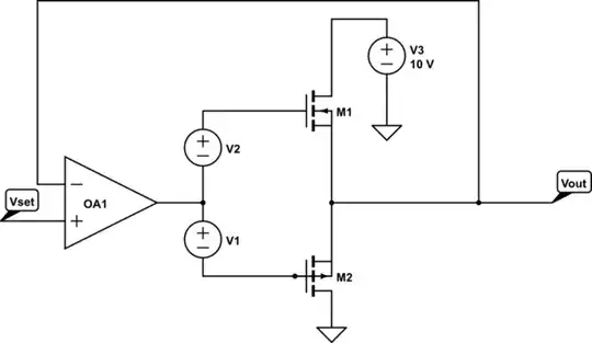
simulate this circuit – Schematic created using CircuitLab

How would you go about biasing a class AB MOSFET stage to reduce crossover distortion at an acceptable quiescent current when threshold voltage is not a well known quantity in practice? Is there any good reference circuit design or article that tackles this?

Lars Hankeln
  • 2,513
  • 1
  • 8
  • 15
  • Vbe multiplier can be the answer https://electronics.stackexchange.com/questions/449914/vbe-multiplier-with-emitter-resistance-cancellation/449975#449975 and this http://buildaudioamps.com/wp-content/uploads/2014/12/AN-948%20IR%20HEXFET%20Linear%20Power%20Amp.pdf – G36 Aug 09 '21 at 15:12
  • 1
    Or take look at this example https://serwis.avt.pl/manuals/AVT2625.pdf (page 2) – G36 Aug 09 '21 at 15:35

2 Answers2

4

Think again about the packages. MOSFETs are almost always used as switches and dissipate very little power. Here you are using them as linear devices and they will dissipate as much power (or slightly more according to threshold voltage) than bipolars.

So, make sure you are using adequate packages and heatsinking to get that heat out ... probably the same ones as those bipolars.

Having got that out of the way, ... biassing. I would suggest adding source resistors (where the emitter resistors are in a bipolar output stage) and using the DC voltage across them as a measure of the quiescent current; allow this to control the bias voltages.

  • How would you know what part of the voltage drop is caused by quiescent current and what is caused by load current? Measuring output current as well? The output current is also expected to have a significant DC component. A schematic or link would certainly be helpful. – Lars Hankeln Aug 09 '21 at 16:24
  • 1
    @LarsHankeln I was thinking a low pass filter would do it (coming from an audio background!) but there's another way : the quiescent current passes through both source resistors, the load through only one.. How to exploit this? Not quite sure, but I think you can take the lower magnitude source resistor current as the determinant. (Measure both, use a diode combiner, low pass filter). I don't offhand know of a circuit, I'm only outlining a design approach. –  Aug 09 '21 at 18:20
  • Thank you. Regarding packages the problem is that I am limited to DPAK or even lower profiles. BJTs in that package appear to have significantly higher Rth,jc. I don't know the reason for that, but that causes higher junction temperatures at the same power compared to FETs. – Lars Hankeln Aug 10 '21 at 03:54
2

Your dilemma is balancing the high side and low side gate voltage, right? I would put two OP amps, one at the high-side, another at the low-side, both are fed back from the output, driven from the same input.

jay
  • 3,781
  • 8
  • 24