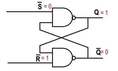
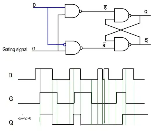
In your first picture, consider the top NAND gate. We know that a NAND gate is such that, if any input is 0, then the output must be 1 (the only way the output of a NAND gate is 0, is if both inputs are 1). Thus, since ~S = 0, then Q = 1, regardless of the second input to the top NAND gate.
Since you now know both inputs to the second NAND gate, it is easy to deduce that ~Q = 0 (both inputs are 1, so the output of the NAND gate is 0)
~S = 0
~R = 1
 Q = 1
~Q = 0
The point of the circuit is that, if you now set ~S = 1, the outputs will not change, because the second input to the top NAND gate is 0 from before (both inputs must be high to make the NAND output change to 0). So now you have:
~S = 1
~R = 1
 Q = 1
~Q = 0
Consider this: What if your initial conditions were switched, i.e. ~R = 0 and ~S = 1? Doing the exact same reasoning as before (except that we now begin with the bottom NAND gate) we find that Q = 0, and ~Q = 1
~S = 1
~R = 0
 Q = 0
~Q = 1
Now the magic happens: we set ~R = 1. What happens? It might help to draw it out, but basically, the outputs will not change due to the same argument we had before; the other input to the NAND gate is already 0, and we need both inputs to be 1 in order to change the output (~Q) to 0. (There is a hint that this would happen, since the circuit is perfectly symmetrical)
~S = 1
~R = 1
 Q = 0
~Q = 1
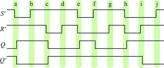
The inputs are the same as before, but the outputs are different! - they remember the previous state.
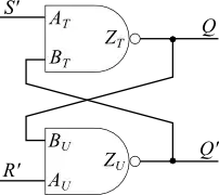
In general, you will never use the case when both ~S = 0 and ~R = 0, because then both Q = 1 and ~Q = 1, which will probably break the logic that is depending on the circuit. That is the point of the two extra gates in your second picture; they protect the SR flip flop so that this particular input will never happen.
(Think of S as "set" and R as "reset" - when both are low, the flip flop remembers the previous state. When S is high, you "set" the output (Q) to 1; when R is high, you "(re-)set" the output to 0. If you try to set the output to 0 and 1 simultaneously, something wrong will obviously happen, so you need to make sure it doesn't happen.)
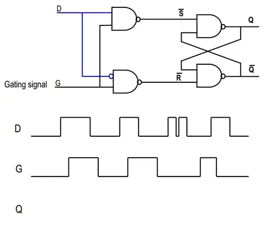
In your second picture, consider the "D" signal: It goes straight into first NAND gate, and an inverted version goes into the second. Now, if D is high, then the second NAND will always output 1, so that ~R = 1. On the other hand, if D is low, then the output of the first NAND will always be 1, so that ~S = 1. In this way, we guarantee that our frightening scenario with the SR flip flop above will never happen, yes?
Now consider the G signal. If G = 0, then both ~S = 1 and ~R = 1; thus, this is the "remembering" state, in which the output stays the same. However, if G = 1 then either ~S or ~R will be low, right? Which will depend on the value of D.
In short, when G is 1, then Q = D, and when G is 0, then Q = Qold