7

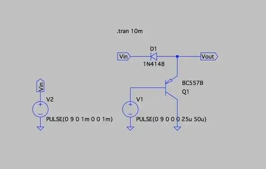
I want to convert a 3V3 PWM (10 kHz) signal to a 0-5V analog DC signal using transistors only (no DAC), if possible. The output logic should be non-inverted, i.e. 0V->0V and 3V3->5V. The time constant of the conversion should be <20 ms.

Which circuit topology could be used to achieve this?

EDIT: I have a 5V supply available.

psmears
  • 678
  • 4
  • 6
Bip
  • 709
  • 1
  • 5
  • 16
  • Can you use an op amp? – Drew Jun 20 '21 at 20:35
  • 1
    Microchip TB3250 - [Using PWM to Generate Analog Output](http://ww1.microchip.com/downloads/en/Appnotes/90003250A.pdf) – ErikR Jun 20 '21 at 20:36
  • @Drew - I could yeah, but I am not sure whether it could be achieved without it. The precision of the conversion could be within 5-10% so... – Bip Jun 20 '21 at 20:38
  • @ErikR - Thanks. That is certainly one way of doing it. – Bip Jun 20 '21 at 20:39
  • 3
    Use a circuit called a **level shifter** or **level translator**. You can do that with a couple of transistors and resistors or use a levelshifter/translator IC for that. – Bimpelrekkie Jun 20 '21 at 21:02
  • 5
    Level convert 3.3V PWM to 5V PWM and then RC filter it to analog? – Justme Jun 20 '21 at 21:09
  • 2
    74HCT family works with “1” >= 2V input on 5V out – Tony Stewart EE75 Jun 20 '21 at 22:11
  • 1
    I agree with Justme and Tony. Use a logic gate followed by an RC. If you absolutely don't want to use any IC, you can still do it with transistors but you will just need a few more of them. A 20ms time constant implies a cutoff frequency of 8 Hz. Should be no problem to remove 10 kHz with an 8 Hz low-pass filter. – user57037 Jun 20 '21 at 22:21

3 Answers3

10

schematic

simulate this circuit – Schematic created using CircuitLab

The 74HCT1G125 buffers and level-shifts the 3.3V to 5V (Vdd should be +5) and the RC filter converts the 5V PWM to analog with a sub-mV p-p ripple and rise time less than 20ms.

enter image description here

Spehro Pefhany
  • 376,485
  • 21
  • 320
  • 842
  • Or a second inverter. – Finbarr Jun 20 '21 at 23:09
  • @mkeith Good catch, thanks. Modified. – Spehro Pefhany Jun 20 '21 at 23:20
  • 4
    I assume the output signal has pretty high impedance, they might want to buffer the final output voltage with a general purpose rail-to-rail opamp – KyranF Jun 21 '21 at 00:50
  • @Finbarr LOL. Sure one more inverter would do. Or 3 more. Or 5 more. But non-inverting buffers are available in the same logic family and footprint so... – user57037 Jun 21 '21 at 01:17
  • @KyranF - I would adjust the output resistance to be <1k and do a compromise over ripple AND/OR increase the switching frequency. – Bip Jun 21 '21 at 19:22
  • 1
    Probably best to buffer the output with a rail-to-rail op-amp. Otherwise the internal resistance of the buffer will start to adversely affect the linearity. But your requirements are very fuzzy so hard to tell. If you drove a pair of MOSFETs with an inverter (or another pair) you could do it directly without a buffer and lower resistors/bigger caps but there would be some other downsides such as some shoot-through current and some ripple due to layout most likely. – Spehro Pefhany Jun 21 '21 at 19:25
  • @SpehroPefhany - 74HCT has the worst case of Vin_h as 3.15 under 4.5V VDD. That seems edgy. – Bip Jun 21 '21 at 20:08
  • 1
    @Bip The datasheet I linked has both 74HC and 74HCT. You'll find the HCT numbers on page 5. For Vcc between 4.5 and 5.5VDC the minimum is 2.0V and typical is 1.6V. Plenty of margin. – Spehro Pefhany Jun 21 '21 at 20:12
  • @SpehroPefhany - gotcha, thanks! Do you have any link where I can read more about the linearity effect that you mentioned when using 74HCT with a resistor in series in <1k range? Thank you. – Bip Jun 21 '21 at 20:35
  • 1
    I suggest simulating it and playing with the values, either in Circuitlab or (as I did) in LTspice (free download). Intuitively, if it charges with one resistance value and discharges with another, the value at mid-scale will be different from 50%. – Spehro Pefhany Jun 21 '21 at 20:37
9

schematic

simulate this circuit – Schematic created using CircuitLab

the conversion is not perfectly linear, but this improves the more that R2 has higher resistance than R1.

M1 is some mosfet that switches at less than 3V

For < 20ms time constant satisfy the inequation (R1+R2)C1 < 20mS

  • Very neat, I may implement something like this! Thanks! – Bip Jun 21 '21 at 06:43
  • Can you please explain this thing about "non-linearity" regarding the R1 and R2? – Bip Jun 21 '21 at 06:51
  • 2
    If we assume that the FET and the signal source are ideal, then the speed of charge is set by R1+R2 but the speed of discharge is set by R2 only. So rather than the mean output voltage being 5V*Th/(Th+Tl) it's 5V*(Th/(R1+R2))/((Th/(R1+R2))+(Tl/R2)). – Peter Green Jun 21 '21 at 16:13
6

Since there is 5V supply available, one solution would be to use a logic gate to convert 3.3V PWM signal to 5V PWM signal, and then RC filter the 5V PWM signal to analog with the requirement of the 20ms time constant.

The logic gate would have to be suitable for accepting 3.3V levels at input while being powered at 5V to provide 5V output. One suitable type out of many is the HCT logic family.

Justme
  • 127,425
  • 3
  • 97
  • 261