5

The typical picture from the pich-off phenomenom assumes that when channel pich-off occurs the density of mobile charge in the region from the pinch-off point up to the drain becomes zero.

This regions is asumed fully depleted and there is present an electric field which sweeps off all the charge that it is injected in this region. In other words, although the density of mobile charge is zero, current can flow through the depletion region.

My question is related to this last specific statement. If the charge density is null, the drift density current is also null by definition since, for intance for a NMOS, the current density Jn = q n mhu E. Obviously, this cannot happens. In this sense, my questions are:

  1. How this effect can be interpretated?
  2. Which charge density supports the drift current?

I have been cosulting several books on the topic, but all of them omit this comment. Maybe is trivial, but any ligh on the topic would be welcome.

The question can be also translated to current flow through the depletion region in diodes.

Regards, Antonio

Antonio
  • 51
  • 1
  • Get Grammarly for English spell-check. Pinch-off is between drain and source at specified Vgs bias increases resistance with voltage from IDSS till Ids=leakage current listed. – Tony Stewart EE75 May 26 '21 at 22:06

2 Answers2

4

Even with no pinch-off formed, a depletion region, free of charges, surrounds both source and drain terminals. The specific resistance of the depletion region, however great, is finite and similar to an intrinsic silicon resistance. Because the depletion region surrounding the source and drain terminals is thin, the series resistances of these terminals are small. Also, as you notice, the depletion region in a semiconductor diode is not an isolator too, otherwise there would be no reverse saturation current in diodes.

Don't be fooled by wedges drawn under gates of FETs in lecture slides. These are not the spatial profiles of charge densities into the bulk depth. In fact, the inversion layer charge concentrates in a mono-atomic layer at the surface that separates the bulk and oxide under the gate. The pictures just illustrate the change of mobile carriers' surface (2D) density along the source-drain direction. The statement about a zero charge carrier density in the pinch-off is (usually tacitly) made about this 2D charge carrier density in the inversion layer, not about the carrier density in the bulk or in the depletion region.

The drain current carriers in the depletion region are the carriers injected into the depletion region from the inversion layer for the most part. Because there are no majority carriers in the depletion region, the injected minority carriers do not recombine and successfully reach the drain.

Your curiosity about charges in the inversion layer and depletion area is an opportunity for you to deeper understand the working of semiconductor devices. Pay attention to the phrase

In 1976 Shockley described Bardeen's surface state hypothesis "as one of the most significant research ideas in the semiconductor program".

in the Wikipedia article https://en.wikipedia.org/wiki/Field-effect_transistor and start with reading this article, or at least the History section.

The surface states is the quantum effect that first prevented the researches from creating the successful solid state device for signal amplification but finally enabled them to create the field effect transistor.
V.V.T
  • 3,521
  • 7
  • 10
  • Thank you very much for your clarification. It has been quite instructive. Now I see that the typical charge density profile picture of the inversion layer, do not represent the total amount of free charge in the channel. Regarding to the depletion region, is there any expression for determining the amount of free charge available in the depletion region? Or equivalently, its resistance? – Antonio May 27 '21 at 06:48
  • 1
    The resistance of the depletion region is on the order of the intrinsic (un-doped) silicon resistance; but the depletion region conductivity per se contributes only negligible part to the total current. The current through the depletion region is almost entirely due to minority carriers injected from the inversion layer. The amount of the injected carriers is governed by the transistor layout and field distribution and only slightly depends on the medium (depleted range) properties. No majority carriers, consequently, no recombination, and nearly all the injected charges reach the drain. – V.V.T May 27 '21 at 09:19
1

example.

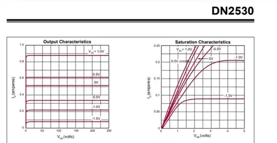
Vgs(OFF) -1.0 to -3.5 V at Id= 10 µA
IDSS 200 mA VGS= 0V, VDS= 25V
12 Ohms at IDSS

Id changes with Vgs between 0 and pinch-off Vgs(OFF) (see plot on right)

N-ch Depletion mode

enter image description here Here Vds is swept with stepped Vgs enter image description here

The depletion channel has the electric field that pinches off on either side of the Vds channel so that drain and source ohmic contacts cannot conduct. The fields are orthogonal and the Vgs channel is highly doped.

The Vt threshold is difficult to control so the tolerances are not reflected in “nominal” plots.

Tony Stewart EE75
  • 1
  • 3
  • 54
  • 182
  • 2
    This doesn’t seem to answer the question. – Adam Haun May 26 '21 at 22:57
  • @AdamHaun still? – Tony Stewart EE75 May 27 '21 at 00:02
  • 1
    I understand the effect of pinch off in the output characteristic, but my question is related to the expression of the current density below: Drift current density (electron): Jn = q n mhu E where, q: electron charge n: charge density mhu: mobility E: electric field According to this equation, the current density should be zero if n= 0, but this not the case for a transistor on saturation. What's wrong in this interpretation? – Antonio May 27 '21 at 05:19
  • The axis of drift current is not the same as the axis of pinchoff in the inversion layer. – Tony Stewart EE75 May 27 '21 at 14:44