Intro
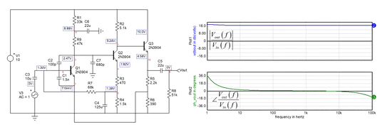
It's a great catch that Verbal Kint made; that schematic. It helps a great deal. There are a lot of details I used to see in these older BJT designs there, including isolation methods I might discuss later on. Also, the NFBs that were visible to me in the diagram you gave have been largely rendered moot in the more accurate diagram. For example, what I imagined as NFB from the middle BJT's (your \$Q_2\$) emitter back to the base of the left BJT (\$Q_1\$) is actually destroyed (shorted out at AC) by a \$125\:\mu\text{F}\$ capacitor in the actual diagram. So it's important to get all the details laid out to avoid misunderstanding.
That said, the DC loop to analyze for the DC operating points remains similar. So I can just ignore the small-signal AC stuff, I think, and just focus on a really easy approach to working out the DC bias details.
Rather than duplicate Verbal Kint's diagram from his answer, I'll just extract the part values and numbers from it, while eliminating the AC bits I don't care about:

simulate this circuit – Schematic created using CircuitLab
One last detail. It took me a few minutes, but I found out that the \$B+\$ supply is \$+24\:\text{V}\$. This feeds a \$270\:\Omega\$ resistor and \$470\:\mu\text{F}\$ capacitor that are not shown in Verbal Kint's diagram. It's the voltage at the capacitor that is \$N\$ in the schematic. Just FYI. (See diagram near bottom, below.)
DC Bias Loop
The DC operating point for this schematic just requires some starting point. Then just walk it around and follow along towards its conclusions.
Let's start with the output, which I've labeled \$V_{\text{E}_6}\$ and work around a simple loop. (Let's assign \$V_\text{CC}=V_\text{N}\$.)
- From \$V_{\text{E}_6}\$ we find that \$V_{\text{E}_4}\approx V_{\text{E}_6}\frac{R_{18}}{R_{17}+R_{18}}\$. The counter-argument to this would be that the emitter current from \$TR_4\$ might upset this simplifying assumption about a resistor divider. But the counter to that counter is that the collector current for \$TR_4\$ is obviously quite small. You only have to glance at the size of \$R_{11}+R_{12}\$ to see what I mean. So we can afford to ignore that distraction and continue on.
- \$V_{\text{B}_6}\approx V_{\text{E}_6} +V_{\text{BE}_6}\$ (the base voltage is about a diode drop above its emitter voltage.) So the quiescent current for \$TR_5\$ is \$I_{\text{Q}_5}\approx \frac{V_\text{CC}-V_{\text{E}_6} -V_{\text{BE}_6}}{R_{13}}\$.
- \$I_{\text{Q}_5}\$ generates an obvious voltage drop across \$R_{15}\$, so we know that \$V_{\text{B}_4}\approx I_{\text{Q}_5}\cdot R_{15}\$. Again, the counter argument here is that \$TR_4\$'s base current causes a voltage drop across \$R_{10}\$. But again that is itself countered by the fact that since \$TR_4\$'s collector current is so small, its base current is then still that much smaller still, and it won't count for more than a few hundredths of a volt. So we can afford to ignore that distraction, too, and continue on.
- \$V_{\text{B}_4}\approx V_{\text{E}_4} +V_{\text{BE}_4}\$ (see similar statement in #2 above.) So from #3 above \$I_{\text{Q}_5}\cdot R_{15}\approx V_{\text{E}_4} +V_{\text{BE}_4}\$ and therefore \$V_{\text{E}_4}\approx I_{\text{Q}_5}\cdot R_{15}-V_{\text{BE}_4}\$.
- From #2's \$I_{\text{Q}_5}\$ and the results from #4, find \$V_{\text{E}_4}\approx \frac{V_\text{CC}-V_{\text{E}_6} -V_{\text{BE}_6}}{R_{13}}\cdot R_{15}-V_{\text{BE}_4}\$.
- But from #1 and #5, find that \$V_{\text{E}_6}\frac{R_{18}}{R_{17}+R_{18}}\approx \frac{V_\text{CC}-V_{\text{E}_6} -V_{\text{BE}_6}}{R_{13}}\cdot R_{15}-V_{\text{BE}_4}\$.
Solve #6 for \$V_{\text{E}_6}\$:
$$V_{\text{E}_6}\approx \frac{\frac{R_{15}}{R_{13}}\cdot\left(V_\text{CC}-V_{\text{BE}_6}\right)-V_{\text{BE}_4}}{\frac{R_{15}}{R_{13}}+\frac{R_{18}}{R_{17}+R_{18}}}$$
I'll let you plug in values and run a Spice simulation for it and then compare results. But the point is that you can get yourself close to a starting point in analyzing the DC operating point for the circuit without a lot of trouble. Just a few steps around a loop. And not very difficult ones, to be honest.
Yes, I've made a few simplifying assumptions. But I also justified them, too. But if you want to spend more time and get a slightly improved result you can include estimates on the emitter current of \$TR_4\$. (Even with say \$20\:\text{V}\$ across \$R_{11}\$ and \$R_{12}\$ that only comes to about \$250\:\mu\text{A}\$ that is added to something close to \$5\:\text{mA}\$ for \$TR_6\$'s emitter current. Perhaps 5%?) You could add that adjustment, if you wanted, and you can also consider the few hundredths of a volt drop across \$R_{10}\$, too. But you wouldn't stray too far for all the added trouble getting there.
And finally, I found this detail on the power supply rail for the circuit:

So the voltage at \$V_\text{CC}=V_\text{N}\$ will be about \$1.5\:\text{V}\$ less than \$24\:\text{V}\$ with just one module attached. Still less, with another module. So I'm not exactly sure of the operating rail voltage for the amplifier stage. But at least you have a rough idea about it.
Small Models??
There's no need for hybrid-\$\pi\$ models here. Well, actually, one could use the hybrid-\$\pi\$ model if they used the large signal version found here. But when someone says hybrid-\$\pi\$ model they almost always mean the linearized small-signal version of the large signal model. They almost never mean the large signal model. Yet it is the large signal model that is the only thing that would work here in figuring out the DC operating point, if you wanted to go crazy. (You'd have to really love the LambertW function if you wanted a closed solution, too.)
The linearized, small-signal hybrid-\$\pi\$ model is for AC analysis. Not for DC operating points.
