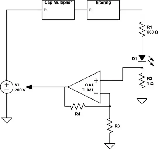
The main theme is: eliminate sources of 1/f as far as possible and limit bandwidth as desired. I suggest the following principal circuit (details added further down):
Low Noise Resistor
The main source of 1/F noise is R1 (at this current level). Therefore, use a resistor with a low noise index. This has nothing to do with its value like Johnson noise, but is a material property. Vishay is well known for their ultra-low noise index "Bulk Metal Foil" resistors, which are a good fit here. The exact value and tolerance is not so critical, but should be selected to give you 200mA. R1 has to dissipate some power, namely (V1)²/R1. This is one of the reason why the reference voltage should be low. If you don't want the metal foil resistors, take a Wirewound. These are also good when both low noise index and high dissipation are important.
How low a noise index is necessary? You'll have to stay below the 1/f noise of the voltage reference, which is usually around 50 nV/rtHz at 1 Hz (coarse figure). At -40dB Noise Index and a reference voltage of 2.048 V, excess noise at 1 Hz is 13.5 nV/rtHz which would be acceptable. However, if the reference voltage is higher, the excess noise rises proportionally. If you are going for a ~7V buried Zener reference and their slightly lower 1/f noise, you are looking to a resistor with better than -50 dB already. This is ambitious ( your typical low noise precision thin film resistor will be in the -30 dB pallpark. Only use parts which have the noise index actually rated.
EDIT: Actually it appears that at such low resistances of well sub 100 Ohm, the Noise Index is less of a problem, as demonstrated in this excellent and exhaustive study. Most parts are well below -40 dB even at 100 Ohms, so lower resistance and higher power will improve this even further. I guess the figures I mentioned above are more usual for ~kOhm sizes resistors.
Low Drift Reference Voltage
Then take a high quality voltage reference, with a low voltage, e.g. 1.25 V. The lower voltage will have less internal amplification and less 1/f noise from the reference IC. Most references have a noise rating in ppm of nominal rms. As you want a current with ~0.1 ppm RMS noise, the same goes for the voltage reference. Out-of-the-box all the low noise band gap references are higher than this in the 0.25 ppm to 0.5 ppm ballpark. In order to reach really low peak-to-peak voltage noise with bandgap references, the lowpassing has to be rather strong. 100kOhm + 1000µF are good values as explained at the end. The exact values of R2/C2 and of the reference voltage are only important if you care about the absolute accuracy of the 200 mA. The diode current will be given by V1 / R1. One part that looks appropriate is the LTC6655CHMS8-1.25. As explained below, the 1/f noise of the reference is what will ultimately limit you.
Alternatively, buried Zener types like the LTZ1000 bring lower proportional noise of below 0.2ppm, but they complicate the design considerably (higher voltage, larger R1 needed with even lower noise index, ovenization). The resistor is far more important anyway, so start with a regular reference and it might be good enough.
Low drift opamp
Build a voltage follower on the reference voltage using a low drift opamp. As feedback point take the current through the resistor. Most low noise bipolar input opamps have low enough drift and low 1/f noise. Just avoid CMOS input opamps like the plague, unless they include zero-drift circuitry. Infact, the zero-drift CMOS opamps are the best for this job. OPA189 is a good part for this job (zero-drift CMOS).
C1 is not so important, but is a good practise when you have a "long" feedback loop with non-linear parts. Especially because the wires connecting D1, might be indeed physically long and create some inductance. C1 then aids with the opamp stability.
The pass transistor is not critical at all
The opamp output steers a pass transistor and this keeps the current through the resistor constant. The pass transistor itself doesn't matter so much. It has to cope with the load current in its linear region. But most of its non-idealities are compensated by the opamp feedback. Any NPN with 0.5A current rating or better will be good. You can use an N-MOSFET too, but you need more voltage at V+ then. Take into account the power dissipation, especially if the V+ is rather high. The pass transistor has to eat all the excess supply voltage.
Add in the laser diode
The laser diode will be between the resistor and the pass transistor.
The regulation of the opamp becomes ineffective at around several MHz for typical precision parts. Beyond this frequency, random noise has to be decoupled passively from D1. So let's add in some filtering:
L1 and C5,6,7 form the main bypass for high frequency noise, with a corner set to ~10 Hz here. You can add more electrolytics to lower the corner frequency further. Typical 10mH chokes rated for a few 100 mA have a series resistance in the 5 Ohm range. This will cause excess noise but this noise is regulated away by the opamp feedback. At higher frequencies above ~MHz, the inductor gets leaky though, due to its winding capacitance. Therefore there is another smaller cap C4 behind the inductor to bypass high frequencies. Together with the impedance R3 it keeps noise up to 100s of MHz away from D1. R3 can be e.g. a ferrite bead generously rated for 0.5 A of higher and can be a normal part with impedance in the ~100 Ohms at a couple of 100 MHz. R3 can also be a resistor. You can use a generic low noise thin film one here. It will have significant excess noise, but this will be regulated away by the opamp feedback. A ferrite bead is probably cheaper and doesn't have to dissipate so much power, and doesn't increase the DC voltage needed to supply the circuit. Finally C3 is the capacitor suggested by you. I don't see much point in it now, but same as C1, it doesn't hurt to have at least footprints for these parts in case they become necessary.
Powering the circuit
The power source for the pass transistor and for the opamp (V+) should be not too noisy. Here is where you can use an LDO to supply that power. But I wouldn't use an LDO for the actual precision current output as suggested elsewhere in this topic. The resistors in integrated LDOs are far more noisy than good discrete parts. You can also use this LDO to power the reference voltage. The Voltage of V+ should be at least the reference voltage + diode voltage + filter forward drop + 0.7V + some headroom that depends on the pass transistor. A safe value will something like 8-10 V. If you want to use an N-MOSFET instead of the NPN, the replace the 0.7V with whatever is the turn-on voltage of the MOSFET.
Expected noise performance
The opamp input current noise does not matter due to the low impedance. Assuming, R1 was selected to have an extremely low noise index and thus negligible 1/f, the two dominating contributions for the peak-to-peak noise are:
- The wideband input voltage noise of the opamp. It will be about 5nV/rtHz for the OPA189. Divide by R1 to obtain 500pA/rtHz. If you set the cutoff frequency of the L-C-bypass round D1 to about 10 Hz, then this will cause 1.5 nArms or 10 nApp in D1.
- However, the more important noise voltage comes from the voltage reference.. This is usually about 1uVpp, and this will re-appear entirely over R1. So it will cause 100nApp by itself with R1 at 10 Ohm if left unfiltered. The filtering around D1 does not really help, because this is 1/f noise which hits us right in our target bandwidth. To reach below 50 nApp total noise in D1, the filtering of V1 has to be strong. By tolerating a lengthy run-up time of the circuit of a few minutes, we can set R2 * C2 to 100s which will substantially cut down on the reference voltage noise. To achieve this high RC product, you can set R2 up to 100k, where its Johnson noise will still not matter compared to the low frequency noise of V1. C2 will be 1000 µF which can still be realized using a smallish Al electrolytic cap.


