12

I've been trying to condense the pure NOR-gate based Apollo Guidance Computer schematics into a more higher level view of the logic elements and came across this interesting piece:

schematic

simulate this circuit – Schematic created using CircuitLab

From this page in the AGC archives.

At first glance, it just looks like a flip flop based on the crossing feedback, but the top NOR gate has 3 inputs, not 2, so it's not a standard flip flop built from 2 input NOR gates.

So then, what exactly is it doing? I'm guessing it's still a flip flop of some sort since it's clearly storing a bit, but what is the extra input on the top NOR-gate for?

TonyM
  • 21,742
  • 4
  • 39
  • 62
stix
  • 344
  • 2
  • 10
  • 5
    Most of us would say that it is **not** a flip-flop, it is a **latch**. – Elliot Alderson May 06 '21 at 19:48
  • 5
    @ElliotAlderson I found myself wanting to refer to it as a latch too, but I found too many internet resources referring to it as a flipflop, including the following: " This distinction is relatively recent and is not formal, with many authorities still referring to flip-flops as latches and vice versa, but it is a helpful distinction to make for the sake of clarity." – stix May 06 '21 at 19:54
  • 1
    There's a more complicated latch in the AGC that has a flaw... have fun: https://electronics.stackexchange.com/questions/452206/how-to-analyze-s-r-latch-circuits/452207#452207 – hacktastical May 06 '21 at 19:57
  • 2
    In case wider context helps, F10B is one of the phases of the 100Hz clock, and TC0 and TCF0 seem to be signals indicating that the current instruction is a TC or TCF (jumps to either erasable or fixed addresses). This appears to be part of the "TC trap", or in modern parlance, a watchdog that makes sure that the CPU is executing a jump at least every few milliseconds. It doesn't matter which of TC0 or TCF0 we get, either one is fine. – hobbs May 06 '21 at 20:04
  • 2
    @ElliotAlderson In the 1960's pretty much any such arrangement of cross-coupled switching elements was know as a flip-flop. The modern distinctions hadn't entered the language. – John Doty May 07 '21 at 13:51

2 Answers2

10

It is an alternate signal for setting the state with the output high.

It could be for example connected to a global signal to set a group of registers to a known value.

Kevin White
  • 32,097
  • 1
  • 47
  • 74
7

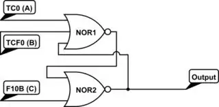
You can add/remove as many additional inputs as you want to both NOR gates. All you have to do is leave at least one input on the gate to close the positive feedback.

An example of such a "1-input NOR gate" can be the simple transistor inverter. I used it to build a transistor RS latch in front of my students many years ago. In 2008, this scenario was implemented in the lab and described by my students in a Wikibooks story.

The figures below show the evolution of this idea or more precisely, the way of drawing. As you can see, the last three figures are equivalent.

Noninverting amplifier

Fig. 1. A noninverting amplifier

Latch by a noninverting amplifier

Fig. 2. Latch made by a noninverting amplifier

Latch by two inverters

Fig. 3. Latch made by two inverters in loop

Latch by cross-coupled inverters in loop

Fig. 4. Latch drawn as two cross-coupled inverters in loop

SRAM cell.jpg

Fig. 5. Latch symmetrically drawn as two inverters in loop (SRAM cell)

Note that all these structures are made by 1-input elements. They are "brutally" driven by applying the input signals to the same inputs where the positive feedback is applied. So there is a conflict between two voltage sources - the circuit outputs and the input sources. The solution is to control the cells by more powerful input sources (as in SRAM)... or to add additional inputs for the input sources (as in flip-flops) to control the cells in a conflict-free way.

RS latch

Fig. 6. RS latch implemented by 2-input NANDs (Wikipedia)

TonyM
  • 21,742
  • 4
  • 39
  • 62
Circuit fantasist
  • 13,593
  • 1
  • 17
  • 48
  • 1
    Indeed. And not limited to 1960's NOR-only logic. I put almost exactly that circuit into an x-ray spectrometer design a couple of months ago. CMOS NAND rather than RTL NOR, but otherwise identical. – John Doty May 07 '21 at 13:57
  • @JohnDoty what did you find about the diffraction pattern of the circuit? – user253751 May 07 '21 at 15:13
  • 1
    @user253751 It's a nondispersive spectrometer ツ – John Doty May 07 '21 at 15:16
  • @JohnDoty oh, wrong instrument. What did you find about the X-ray spectrum of the circuit? – user253751 May 07 '21 at 16:03
  • @user253751 I didn't say I put the circuit into an x-ray spectrometer. It's part of the *design* of an x-ray spectrometer. And my collaborator hasn't built it yet. – John Doty May 07 '21 at 16:32
  • 1
    @JohnDoty darn, I skipped the word "design", otherwise I thought it was a good joke – user253751 May 07 '21 at 16:42
  • @JohnDoty Don't laugh, back in the early 1960's we physics geeks were trying to analyze cement by small angle diffraction of x-rays through a powder sample. – richard1941 May 13 '21 at 18:56
  • @richard1941 Powder diffraction is still a technique. – John Doty May 13 '21 at 19:14