The popularity of common-collector output stages comes from the ease of use: particularly biasing, and insensitivity to load condition.
Also to fill out the list: common-base requires full drive current (input current is slightly higher than output) -- something of a non-starter. So the only viable alternative is common-emitter.
CE has substantial voltage gain, and a high output impedance. Meaning, the gain is high, but it's also proportional to load impedance (which is much lower than the amplifier's intrinsic source impedance, thus dominating, and the equivalent circuit looks like a Norton source, a current into a load impedance).
On top of this, we need considerable gain in the input stage, to get sufficient overall gain to keep distortion low and bandwidth high. (The fact that amplifiers regularly have < 0.01% THD is a direct consequence of having loop gain of several thousands -- millions, even.)
A consequence of high gain, is low bandwidth at that gain. A CE or CB stage's bandwidth is limited by capacitance at its output: at DC, Early effect and load resistance dominate, but at AC, node capacitances quickly take over. And with that capacitance, comes a 90° phase shift. (A resistive-loaded 2N3904 in CE, might have a gain of 10 up to a couple MHz, then fall off above there; a CCS-loaded one might have a gain of 2000, but rolling off at say 10kHz -- it has the same GBW (gain-bandwidth product), just different gain at DC. An op-amp might have a gain of 10^5 at DC, dropping off at single digit Hz -- but still a GBW of some MHz!)
Too much phase shift stacked up, causes oscillation. More than 180° means the feedback signal comes in positive rather than negative, thus increasing rather than decreasing the signal. We must cut the loop bandwidth below the point where this happens. If we have two stages cascaded with say gain = 100 and GBW = 1MHz, then the total phase shift is close to 180° above 50kHz or so. (Note they roll off at GBW/gain = 10kHz, at the same time transitioning from 0° phase shift at DC-1kHz say, to 45° at 10kHz, to ~90° at >>10kHz. See standard Bode plots for a visualization.)
If we have two or three stages cascaded, with high gain and thus significant phase shift at signal frequencies, we simply get an oscillator. We need to reduce the phase shift (which is to say, increase GBW) of at least one such stage, within the bandwidth of the other, until stable loop gain and phase shift is met.
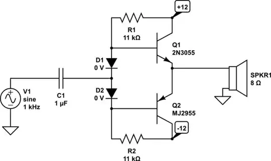
Conventional amplifier designs use a three-stage cascade: the input stage (typically a differential pair) has high gain and bandwidth, so that it contributes little phase shift within the design bandwidth; the middle ("VAS" volt-amp stage) has high voltage gain (typically near rail-to-rail), adequate drive current for the output, and modest bandwidth (it sets the "dominant pole" limiting loop gain and roll-off); and the output is a simple emitter follower, taking the voltage from the middle stage (which is easy enough to cover) and amplifying its current capability (enough that the output voltage gain is fairly independent of load). Thus, phase shift is modest within the required bandwidth, and compensation can be tested and set fairly easily, without much trouble from pathological load impedances.
Finally, a CE output stage is difficult to bias. You can set quiescent current alright, but the transistors are pulling from opposite rails, no communication between each other, just a solid tug-of-war between their collectors. It's very easy to design a circuit which wastes a lot of current on shoot-through (especially dynamically, as it typically takes more time for one side to turn off (storage time) than the other to turn on). And, as they heat up, you need to somehow sense that current and throttle them down, or compensate beforehand (by setting bias voltage and thus current, lower as temperature rises).
Whereas, these are all very easy to do in the complementary emitter follower design: a fixed voltage between bases, will set the bias voltage, and by making it proportional to a diode drop (stack of diodes, or a "Vbe multiplier") and thermally coupling those junction(s) to the output heatsink, it tracks output transistor Vbe just fine. A little emitter resistance sets the current, and you're done.
The flip side of this is shown in strong relief, when it's unavoidable: low-dropout (LDO) regulators are of such a design, that is, an error amp followed by a common-emitter/source stage. They are notoriously sensitive to load impedances, typically demanding output bypass capacitance, with ESR, in a certain range. (Only in recent decade(s) have designs improved to the point where they are stable with very low ESRs (ceramic capacitors), as well as eliminating other pathological behaviors like ground-pin current draw in dropout -- a classic issue of PNP types, and solved with more careful design, or with CMOS based designs.) Early rail-to-rail op-amps suffered similar problems; some types were completely unstable with any kind of capacitive load. Robust types (from both product families) are widely available today, so it's less of an issue now, but always something you need to be wary of when selecting a new part.
Note that regulators are just half an amplifier: typically they only source current, not sink it, so they actually have the added complication that bias current is externally controlled (load current), and thus also falling slew rate depends.
How did they solve the problem? One way is to put all the gain at the output. Construct the output stage, not as a single CE transistor, but a compound "super transistor" with a wide(r) bandwidth gain/driver stage in front, while still looking like a transconductance amplifier overall (that is, some input signal voltage is transformed to some proportional output current). This pushes the gain node (and thus the dominant pole) straight to the output pin itself: while this makes the amplifier indeed maximally sensitive to load variation, compensation is still alright, as long as the phase shifts in the rest of the circuit are low enough. Basically, the input and driver stages need to perform that much better. So, it's not ideal, kind of suboptimal. (They have many hacks, to save on current consumption, to short-circuit the phase shift through certain paths (feed-forward), nonlinear adjustments (slew rate boosting) to fake having higher speed, etc. Lots of stuff I don't know about, too, tucked away inside patents or trade secrets.)
In short, these are techniques that aren't very useful for audio amplification purposes -- it takes tons more transistors to implement (which cost approximately zero on chip!), while you have more than enough voltage available (30V+) that losing the 1-2V drop in a conventional design is inconsequential. So these rail-to-rail designs aren't worth the trouble.


