0

Background

I'm designing a LED controller based on a Teensy 4.1, some AD9833 Function Generators and some TLC5948 LED Drivers. I'm aiming to make an instrument of sorts, specifically a POV display that transmits a series of musical notes via light to a solar panel + amp. I know the music won't exactly be visible due to the relatively high frequency, so I'm going to add that signal on top of an image signal. Thanks to the help of glen_geek on my question here, I decided to use AD9833s to generate notes that I'll read in through ADC on the Teensy and use that data to adjust the LED PWM signals on the TLC5948s.

Problem

I'm wondering if a more experienced PCB designer can tell me what I'm doing wrong or if there's another way to achieve my goal.

This is my first attempt at a PCB, and I've hit a wall. I'm not really sure how I would go about routing the TLC5948s to the LEDs neatly. I added a picture of my first attempt, and to me it feels really clunky, messy and wrong. I could only get everything connected using 4 layers. I've tried looking up layouts for LED arrays/matrices for inspiration but I can't find anything that isn't designed for strobing the LEDs (i.e. common row/column connections). I'm not opposed to strobing but I haven't found any LED drivers that offer that as a feature and I'm worried that'll add audible noise to the music if it's not fast enough (ideally it should be above 20Khz so people can't hear it). Does anyone know if there's a cleaner/easier way to route this or an IC that can handle strobing at high frequency? This has been answered by @Justme.

Feedback

I'm also looking for feedback, both on the circuit design and the PCB layout. Two questions I have are:

  1. Is there any way to make this smaller?
  2. Is it ok that I cross some of the LED lines with clock signals? If not, is there a fix?

I tried my best to research the basics like decoupling capacitors and keeping analog/digital ground separate, etc, but if I've missed something else I'd love to know about it. Also, any ways to make the board more compact would be appreciated as well.

Thanks so much in advance!

Revised PCB Design #1

I made the following changes and reattempted the routing thanks to the suggestions from @Justme.

  1. Use 3.3V for RF, AD9833s, and TLC5948s
  2. Use 3.0V for Hall Effect Sensor (since output can be Vcc +0.3 and Teensy is only rated for 3.3V)
  3. Change pin order on the TLC5948s to consecutive pins
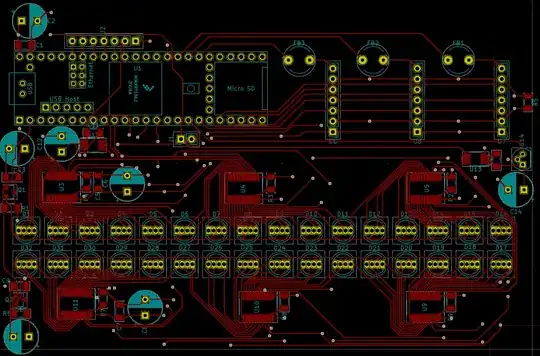
Improved Design Pictures

Top Layer PCB Bottom Layer Main Circuit Schematic LED Array Sub-circuit Function Generator Sub-circuit Hall Effect Sub-circuit

wootie11
  • 45
  • 5
  • Would it be simpler to route three concecutive chip outputs to a single LED, instead of having separate R chip, B chip etc? – Justme Apr 06 '21 at 15:31
  • @Justme That's a good idea, I didn't even think of that! I'll give it a try. – wootie11 Apr 06 '21 at 15:39
  • How much is VDD? – Justme Apr 06 '21 at 15:40
  • I was think of using another 5V+ supply for VDD. – wootie11 Apr 06 '21 at 15:42
  • Do you think the LED driver chip will work with 3.3V logic levels when powered from 5V? I assume the MCU runs at 3.3V. – Justme Apr 06 '21 at 15:58
  • Also make sure the MCU can tolerate inputs larger than 3.3V so it does not get damaged, as many items sent to MCU are powered from 5V (hall sensor, LED_EN pullup...) – Justme Apr 06 '21 at 16:03
  • Ah shoot, you're right! I just reread the datasheet and Logic HIGH is Vcc... Thank you for catching that. The datasheet says that it can run at 3V, so I'll update my schematic. I just noticed the recommendation for VDD is 10V, too. – wootie11 Apr 06 '21 at 16:06
  • @Justme I've updated the schematic + PCB – wootie11 Apr 07 '21 at 00:03
  • The sdcard might bump into the FB. Your power tracks are way too thin - you want low inductance as well as low resistance. Not sure what your FB are supposed to do or what type they are. As well, the split plane is suspect. I think your design will not fly - at least not quite the way you want it to. – Kartman Apr 07 '21 at 00:23
  • @Kartman What would you recommend as a trace width? The ferrite beads are to help with EMI, I read that switching a large amount of current quickly (like with the LEDs), would cause some pretty serious EMI which can affect the analog readings from the AD9833s. I also thought I should aim to keep analog and digital ground separate, but I could be applying the information wrong. https://electronics.stackexchange.com/a/186206/279687 – wootie11 Apr 07 '21 at 00:31
  • @Kartman Do you mean the overall design won't fly or just the PCB? – wootie11 Apr 07 '21 at 00:32
  • @wootie11. Circuit wise, ferrite beads aren’t what you need - a simple RC network would be better methinks. PCB wise, the split plane is not what you want, track sizing and mech details need attention. – Kartman Apr 07 '21 at 01:20
  • @Kartman Just out of curiosity when would I need ferrite beads? Also, if the PWM signal I'm worried about is 33MHz, I'm assuming I'd find R and C from f = 1/(2*pi*R*C)? I'll edit the split plane, track sizes and SD card slot interference, thank you for the feedback. – wootie11 Apr 07 '21 at 02:16
  • You’ll need to be real careful if you’ve got 33MHz signals being distributed. You’ve got a zillion electrolytic caps- they won’t do much for you. You need 100nF bypass caps on your tlc5948 chips close as possible with low inductance tracks. You need to ensure the 0V pins go to the groundplane via the shortest route. There’s going to be lots of high freq current in the led supply, so use thick tracks and bypass caps. Add series resistors on the high speed gpio incase you have signal integrity issues. I’d lean tiwards a 4 layer pcb. The cost impact is minimal – Kartman Apr 07 '21 at 03:27

0 Answers0