What are the structural differences between Serial NOR Flash and Parallel NOR Flash? If there is a structural difference , then What are the differences between Serial NOR Flash and Serial NAND Flash? I can't seem to get the resource for this particular question from Googling
Asked
Active
Viewed 2,358 times
3
-
Reverted to the original version with its mention of search attempts, as the user deserves credit for making an effort to research this question themselves before asking it. Hopefully there will be fewer downvotes now. – Chris Stratton Jan 23 '13 at 17:00
3 Answers
4
Wikipedia: Flash memory has a pretty good explanation of the structural difference between NOR flash and NAND flash.
NOR flash:

-- NAND flash
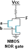
Both kinds of Flash memory use floating-gate transistors. To read out a word, other stuff on the flash chip drives the selected word line to a "small" positive voltage. When the floating gate is charged with electrons, it shields the transistor from the word line enough that the transistor stays OFF. So the resistor pulls the bit line HI, and the CPU sees a one (1) bit. When the floating gate is erased, even that "small" positive voltage on the word line is enough to turn ON the transistor and pull the bit line to LO, overpowering the resistor, and the CPU sees a zero (0) bit.
NOR flash connects those transistors in a NMOS NOR gate. To avoid interfering with the selected word line, other stuff on the flash chip sets the non-selected word lines to GND (turning their transistors off).
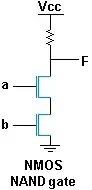
NAND flash connects those transistors in a NMOS NAND gate. To avoid interfering with the selected word line, other stuff on the flash chip sets the other word lines to a "larger" positive voltage (turning their transistors on).
The pull-down path from the bit line to GND goes through many transistors in a NAND flash. The pull-down path goes through only one transistor in NOR flash. So NOR flash can be significantly faster than NAND flash (when built from equivalent transistors). (But even NAND can be faster than a spinning hard drive).
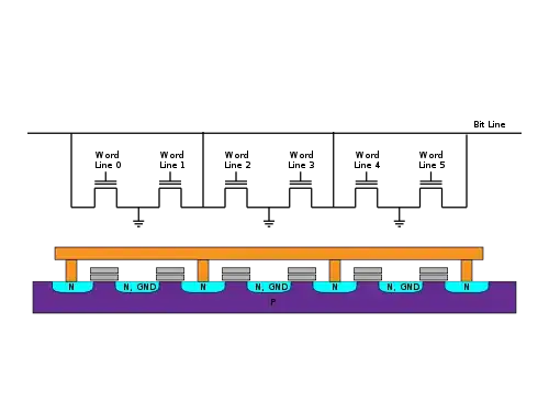
As you can see from the purple chip cross-section, the NOR flash requires many more contact vias from the bit line down to the transistors. Because NAND flash does not need those vias, the physical layout of NAND can be packed significantly less area per bit. So NAND flash can cost significantly less than NOR flash (per bit, and when built from equivalent transistors). (But even NOR flash costs less per bit than DRAM).
Both parallel and serial off-chip interfaces are possible with either NAND or NOR flash.
Execute-in-place applications (XIP) execute directly out of Flash. All the bits of the instruction need to be fetched every instruction cycle, so such applications tend to use parallel NOR flash.
Solid-state disks (SSDs) tend to use parallel NAND flash chips.
Flash configuration memories are usually serial Flash chips. I think I've seen both serial NOR flash and serial NAND flash in this application.
(The pull-up is usually not a literal resistor. The details didn't seem relevant here.)
davidcary
- 17,426
- 11
- 66
- 115
-
I read the article, but I don't understand certain aspects. I can understand that the random read access time of NAND flash would be much longer than for NOR flash, but I don't understand why it would be limited to serial access. The flash chip is going to be a 3d matrix (rows by columns by transistors in each string); at any given time, one can only access one row in a matrix, and one transistor per string, but is there any reason other than external pin-count limits why one should not be able to simultaneously read e.g. transistor #5 in each string on every column of row 28? – supercat Jan 23 '13 at 18:05
-
@supercat: I, too, am mystified. My understanding is that most SSDs use parallel NAND flash chips. Therefore parallel NAND flash chips exist. Therefore NAND is not "limited to serial access". How could I fix my text (or the Wikipedia article) to fight this common misunderstanding? – davidcary Jan 23 '13 at 21:06
-
I don't know. I suspect the main issue is that the long random access times inherent to a NAND-flash array have led chip designers to optimize their interfaces for sequential access; even if it were possible to design a chip which allowed a 5us on-chip random access time and a 20ns on-page random access time, that wouldn't offer much advantage over simply having a 5us random access time and a 20ns "fetch next byte" time. Indeed, the sequential scenario may be faster if data from one page can be clocked out while the next page is read from the array into some latches. – supercat Jan 23 '13 at 21:20
-
1BTW, I wonder what the relation between pages, erase-blocks, and transistor-strings is. I wonder if a "page" represents (once represented) one transistor on each of a whole bunch of strings, and an "erase block" represents a bunch of complete strings? – supercat Jan 23 '13 at 21:22
-
1@davidcary I do understand the structure of NAND and NOR ('parallel connection of cells closely resembles to the parallel connection of transistors in a CMOS NOR gate, that's how it derives the name as NOR flash. In NAND-flash, cells are connected in series resembling a NAND gate, and so the name. The series connection prevents the cells from being programmed individually. These cells must be read in series.') Source:[HERE](http://www.eeherald.com/section/design-guide/esmod16.html) That's y after reading this i though there should be "structural" difference in Serial and Parallel NOR Flash – pjamu Jan 25 '13 at 09:55
3
Serial flash uses serial bus to write and read the data from the device. Popular serial buses include I2C and SPI. Serial signaling involves address, data and control signals on 2-3 wires.
Parallel flash uses parallel 8 Bit I/O or Bus to write and read the data from the device. Parallel signals needed are Data bus (usually 8 bit), address bus (depends on device density) and control bus (en, oe).
I could have added more details but the question is too generic, hence generic answer.
Chetan Bhargava
- 4,612
- 5
- 27
- 40
-
1Thanks, I'm new to this technology and I thought the differences were present in the cell structure.. That's why my question included NAND flash which should be confusing to look at. – pjamu Jan 23 '13 at 06:34
-
Cell structure can be explained by memory designers. I have worked in a memory company and usually the memory circuit designers don't discuss internals on newsgroups. Such questions can also answered by Si technologists (usually PHD guys) – Chetan Bhargava Jan 23 '13 at 06:44
-
Now I know that the "internal structure" or so, as i called it, isn't the problem at all.. Your answer was just what I was looking for.. As I said I'm new to this tech, & I didn't even consider taking I/O access type in to account. – pjamu Jan 25 '13 at 09:45
2
I don't know what you mean by structural - if you mean the internal structure, I have no idea.
Yet, the main difference between serial and parallel NOR flash is the way the memory is accessed. Serial NOR Flashes are accessed via SPI, therefore having a low pin count whereas parallel NOR flashes are accessed via the usual data/address bus.
Check out the following:
Tom L.
- 7,969
- 1
- 19
- 34
-
Yeah I meant the cell structure( I thought the differences should be in this level as the low pin count I'd read about already didn't explain why it's "serial") Now that i learnt that it's SPI accessed, i can understand the interface differences. Thanks anyway.. – pjamu Jan 23 '13 at 06:37