The grounding on this design is very important. To achieve a good grounding, one should create a ground return path so that the "power signals" come back to their source on the same path they go.
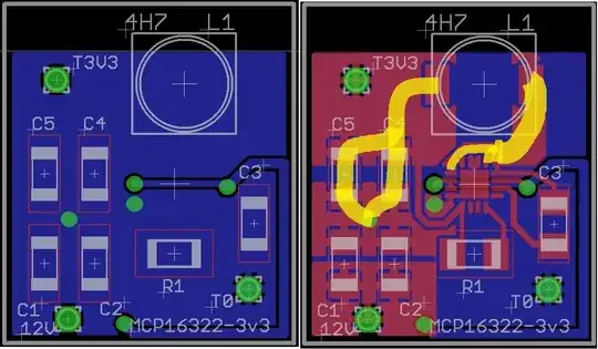
If we were to categorize these power signals, we could separate them into two groups. "Quiet" power signals and "Wild and Noisy" power signals. As I have tried to explain about the noisy power signals in this answer, these signals must be taken of great care. In a typical non-synchronous buck converter, these signals include the ones which have a big change in current or voltage in-between the two cycles of buck converter. Have a look at the drawing below;
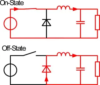
As you can see wild signals are the ones which change color. These include the path that includes the diode, and also the path that includes the input capacitor and switch. In your configuration, which is a synchronous buck converter, everything is the same, except you change the diode with an another switch.
Luckily these switches are integrated in the chip you are using. So that should give a big relief when laying out the PCB.
Coming to your 3rd edition of the design, let's highlight these paths.
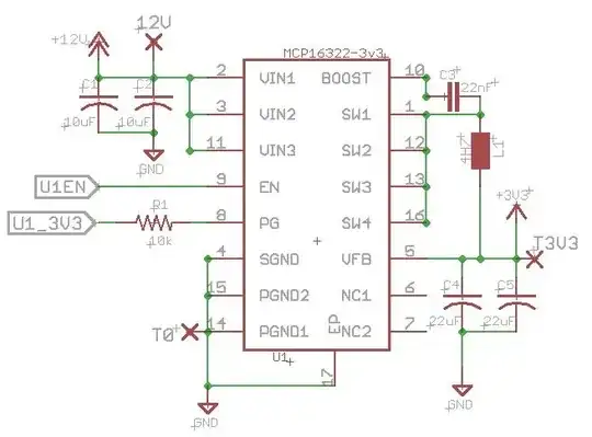
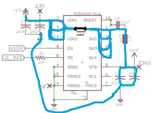
When the upper switch is ON, the power will come from the source, go to your input capacitors C1 and C2, and then go into Vin pins of the IC, which are 2,3 and 11. Then, the power will exit from pins 1, 12, 13 and 16 and go to the inductor, then it will go to the output capacitor and then to ground, and it will try to return back using the same path.
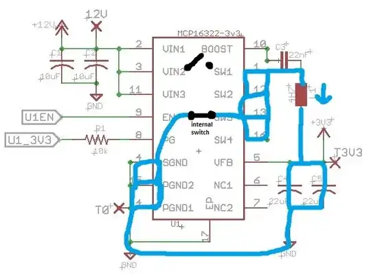
When the upper switch is OFF, there is energy stored in the inductor when the switch was ON, this power in the inductor start flowing from the inductor go to the output capacitor, go to ground, flow back to PGND pins of the IC which are 14 and 15, then it will exit the IC from the pins 1, 12, 13 and 16 then go back to its source, that is the inductor.
In the schematic you draw, here are the two states of the converter:
ON State:
OFF State:
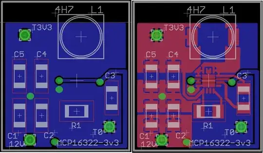
In the PCB you laid out, here is the two states of the converter:
ON State:
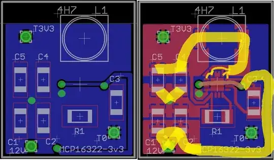
OFF State:
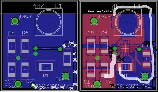
I am very puzzled about the return paths of the signals here, so if anyone has an opinion, I would be glad to hear. But basically, assume that the return paths are right under the trace. If we assume that, then there is no obstacle on the way back to home.
What can be done?
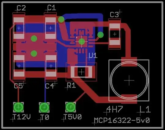
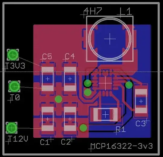
I see that your design is very similar to the reference design on the 22nd page of the datasheet, except you have routed Cin differently. Also, you have routed R1's connection to the 3.3V rail differently. Connect R1 to 3.3V rail just like they did in the reference design. Then, you will have room to connect Cin to the IC with a shorter trace. I have tried to explain in below picture. You can increase the number of vias which will bring better (lower impedance) connections..
Good article from TI: http://www.ti.com/lit/an/snva054b/snva054b.pdf
Sorry for the unnecessarily long post.