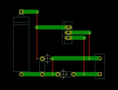
This is a non circuit, but shows my attempt to use KiCad for strip board design. It's actually quite easy if you stick to a mental plan of using the bottom horizontal copper layers as the strips, and the top layer as vertical jumpers. When ever you see two copper strips end to end (the green ones) you insert a cut /break /drill symbol so that you can break the track at that point. That's the yellow cross (which is actually an alignment symbol). You might create your own, that's actually quite easy too.
In detail, you start laying a track at a component pin on the lower copper layer. Click and then go horizontally for a bit. Then click "V" for via. That automatically switches to the top layer and then go vertically. Click "V" again and another via is introduced and you will be switched back to the bottom layer. Then continue to the next component. If you want to finish at a point along a copper strip instead of a component pin, you add a via and end the track there.
The component placement just needs to allow for the majority of the connections running horizontally, otherwise you end up with more jumpers than copper strips! I guess that's okay too, but then you might as well use one of those prototype boards without any strips at all. Also, make sure that you have the grid set to 0.1" to match the pre drilled holes in the board.
The other beauty of this technique is that you can print off the component silk screen. Print in on to paper and stick it onto the strip board. You then have an ersatz silk screen to aid in component placement if you poke the leads through the paper.
[Can't speak for Eagle though. My recommendation would be to dump the niche tools like VeeCAD and even more esoteric ones. They will have little on line support to help you, slow development /bug resolution and will always be playing catch up with bigger tools. This is not a treatise on EDA tools, but with CERN support for KiCAD, there seems to me to be no reason for newcomers to begin with Eagle.]