1

What I'm trying to do?

I'm making a constant-current source based off an existing design. The specs of the existing design are:
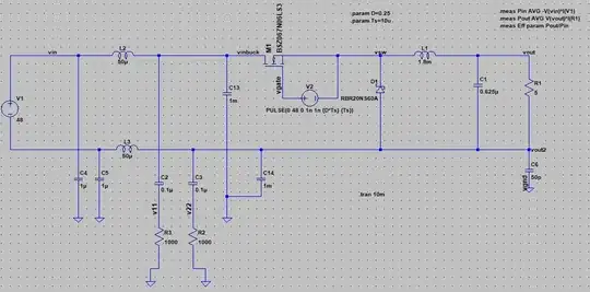
Existing Design

The design is of a constant current source capable of outputting 4-20mA output current from an input voltage of 0-2V.

enter image description here

The Problem

The problem is when physically making the circuit, the output of this circuit is stuck at 56mA irrespective of input.

I cannot find/contact the original author of the schematics to discuss the problem and its up to me to figure this out.

The simulations also show the same results as in reality:

enter image description here

enter image description here

Simulation Findings

Input: Sinusoidal Wave of 0-2V peaks of frequency 1 per second
Output Current: Constant current of 56 mA
Output Voltage: 13.6474V with small ripples with amplitude in microvolts.

PMOSFET Info

enter image description here

V(Gate)   : 23V
V(Source) : 14V
V(GS)     : 8V

Question

1) Where should I start looking for issues?
2) What is the name of the op-amp configuration being used in the second stage? I do know that the 
   first stage is a voltage follower.

enter image description here

EDIT 1: Resolving whether PMOSFET Symbol is correct

I have inverted the MOSFET just in case and the result is a little better but still not close to expected. Don't know whether inverted helped or made it worse.

enter image description here

Mohsin
  • 107
  • 1
  • 12
  • The connection to the inverting input of U2A in your design does not match U4A in the old design. – The Photon Mar 10 '21 at 19:00
  • @ThePhoton thanks for spotting that. That error was already fixed by the time I ran the simulation so the results are still valid. Its just an old screenshot, I'll update it. – Mohsin Mar 10 '21 at 19:05
  • In the simulation, does the DC operating point make sense? Are all the op-amps working in their linear regions, and the FETs in saturation? – The Photon Mar 10 '21 at 19:07
  • I'm sorry I'm just a beginner and am currently googling to find out DC operating point of these op-amps. The FET is in saturation with Vgs of 8V (sorry if I'm wrong about this). See edit as well, the PMosfet section. – Mohsin Mar 10 '21 at 19:16
  • 2
    I think your PFET (Q2) is upside down. The source should go to the positive supply side. – Aaron Mar 10 '21 at 19:58
  • @Aaron, yes. Strange symbol on the original circuit, with the gate exactly in the middle. – devnull Mar 10 '21 at 20:05
  • @Aaron and vangelo I have inverted the mosfet and added results as Edit 1 at the end of post. Please check. – Mohsin Mar 10 '21 at 20:12
  • The original part (Q5) is drawn as a P channel JFET, which is an depletion mode device. But they are also using the same symbol type for the 2n7002, which is *not* a JFET. The symbol for Q2 that you have is for an enhancement type MOSFET. – Aaron Mar 10 '21 at 20:43
  • There's something strange going on with the P-MOS in your simulation. Your voltage notes show it with Vgs of at least -19V, but it's barely conducting. You have an an appropriate simulation model selected there? – brhans Mar 10 '21 at 21:07
  • I re-created your schematic in Circuit-Lab and it simulates fine there ... – brhans Mar 10 '21 at 21:14
  • @brhans can you please share simulation link please – Mohsin Mar 10 '21 at 21:39
  • 1
    @Mohsin could you please confirm that the original circuit is supposed to provide 4mA at the output when the input = 0V? – devnull Mar 10 '21 at 21:45
  • @vangelo I found this strange as well but the schematic states that it does. If you look close to output label – Mohsin Mar 10 '21 at 21:47
  • @Mohsin In the output yes, but where is the DAC range stated? To be more explicit: for a 0V input the output should also be zero (or very close to this). – devnull Mar 10 '21 at 21:50
  • I'd double check pins of devices to model. For example pin number doesn't match for 2N7002 and datasheet (might be ok). For Q2 symbol and label doesn't match; PMOS current should go source to drain [link](https://electronics.stackexchange.com/questions/3599/basic-p-type-mosfet-question#:~:text=1%20Answer&text=For%20an%20N%2DChannel%20MOSFET,switched%20from%20source%20to%20drain.) Also for q2 I've heard voltage to current converter as a name, see [link](https://terpconnect.umd.edu/~toh/ElectroSim/Booster.html) – Ernesto Mar 10 '21 at 23:07
  • @Mohsin - posted as an answer because I can't figure out how (or if it's possible) to just post a link without creating a Circuit-Lab account. – brhans Mar 11 '21 at 00:20

2 Answers2

1

Your circuit simulates fine in Circuit-Lab.

schematic

simulate this circuit – Schematic created using CircuitLab

The comment from vangelo on your question is also applicable - for 0V in you cannot get 4mA out with this circuit.
It's not a 0-2V to 4-20mA converter, it's a 0-2V to 0-20mA converter.

brhans
  • 14,373
  • 3
  • 34
  • 49
0

The LED and the diode in series seem to give some headroom for the op. amp. since the original one can't reach V+ and that also applies to the inputs. Depending on the op. amp. you use, you may have problems.

If R10 was connected directly to +VF the input voltage of the third op. amp. would be very close to +VF (from +VF to +VF-2).

This is what you should expect for 1V DC input:

enter image description here

devnull
  • 8,447
  • 2
  • 15
  • 38