There is an excellent application note by nxp that explains this clever level translation circuit.
See section 2.3 of http://ics.nxp.com/support/documents/interface/pdf/an97055.pdf
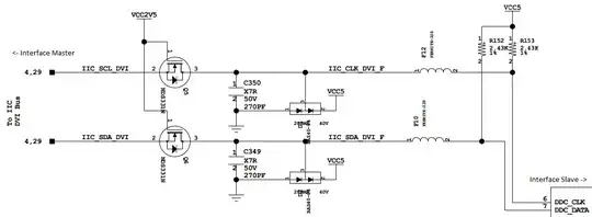
Since the least understood part is how a low goes from the right (higher Vdd) to the left (lower Vdd), I'll explain that first.
Basically when the right hand side (slave in this case) goes low, the parasitic diode pulls the left side down enough that Vgs > Vth, so the mosfet becomes conducting and the left side can be pulled down to the same low voltage as the right side via the mosfet's channel (so not just down to a diode's drop).
That last detail is what makes the circuit clever. It is easy to forget that a mosfet can conduct both ways when turned on, after realizing that it is the parasitic diode that will help turn it on.
What follows is just an excerpt of the aforementioned application note, as a reference.
For the level shift operation three states has to be considered:
• State 1. No device is pulling down the bus line and the bus line of
the “Lower voltage” section is pulled up by its pull-up resistors Rp
to 3.3 V. The gate and the source of the MOS-FET are both at 3.3 V, so
its VGS is below the threshold voltage and the MOS-FET is not
conducting. This allows that the bus line at the “Higher voltage”
section is pulled up by its pull-up resistor Rp to 5V. So the bus
lines of both sections are HIGH, but at a different voltage level.
• State 2. A 3.3 V device pulls down the bus line to a LOW level. The
source of the MOS-FET becomes also LOW, while the gate stay at 3.3 V.
The V rises above the threshold and the MOS-FET becomes conducting.
Now the bus line of the “Higher voltage” section is also pulled down
to a LOW level by the 3.3V device via the conducting MOS-FET. So the
bus lines of both sections become LOW at the same voltage level.
• State 3. A 5 V device pulls down the bus line to a LOW level. Via
the drain-substrate diode of the MOS- FET the “Lower voltage” section
is in first instance pulled down until V passes the threshold and the
GS MOS-FET becomes conducting. Now the bus line of the “Lower voltage”
section is further pulled down to a LOW level by the 5 V device via
the conducting MOS-FET. So the bus lines of both sections become LOW
at the same voltage level.
The three states show that the logic levels are transferred in both
directions of the bus system, independent of the driving section.
Some advantages of using this single transistor design are cost, simplicity, and least dependence on a specific vendor. Bidirectional transmission gates will get you a bit of extra speed, but in the case of I2C it would most likely be unnecessary.