9

I'm working on my first major schematic design and would really appreciate some feedback on the analog side of the 1000BASE-T Ethernet interface. I'm mostly concerned about the analog line termination and the isolated supply of the analog signals and separate ground plane. This is the analog side. I've used the same center-tap voltage as the phy analog in, and isolated the gnd using a ferrite-core inductor.

enter image description here

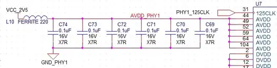
Here's the analog power into the PHY (enough decoupling caps? I used as many caps as input power pins):

enter image description here

I'm a bit concerned about the fact that the phy (88e1111) doesn't have a dedicated analog GND, so I would assume that the analog outs are relative to the global gnd. Doesn't this mess up my ground isolation external to the device?

I would also appreciate it if you could critique my schematic layout, a client is going to see this and I want it to be perfect!

stanri
  • 5,352
  • 2
  • 27
  • 54
  • The single point connection of the PHY analog GND will be joined to the rest of system GND under your PHY in the layout. If the L10 ferrite can bridge in the analog PHY power very near that same point all the better. – Michael Karas Jan 10 '13 at 14:31
  • 2
    Remember to check if Your PHY has current or voltage outputs. E.g. Micrel 1Gbit PHYs require transformers designed for current outputs. Also check if your PHY doesn't have 49.9ohm resistors embedded inside, because most of PHYs now have them. – Tomas D. Jan 10 '13 at 15:40
  • Props for nice, readable schematics. – Connor Wolf Aug 12 '13 at 20:02

3 Answers3

8
  1. Where is the transformer? How exactly the termination is done, and what impedance it needs to be is a function of the PHY's requirements, which then dictate a particular transformer configuration. Since the transformer is integral to termination, we need to see it. You should really show everything from the PHY all the way to the RJ-45 jack.

    Your terminations look correct assuming this PHY requires transformers with 1:1 ratio.

  2. Do you really need to terminate all 4 pairs? Ethernet data is carried on RJ-45 pins 1,2 and 3,6. The other two pair aren't used for data but could be used for POE. If you intend to use POE then you definitely don't want the 100 Ω between pairs. If not, just leave them floating. Why are they connected to the PHY at all? Exactly what type of ethernet are you implementing here?
  3. I really don't like disconnecting the PHY ground and main ground with a inductor, as you do with L9. I can understand you want to keep the PHY's high frequency power/ground current off the main ground plane. It looks like you have isolated the PHY's power nicely with L10 and bypass caps C69-C74. All you need to do is connect all the PHY grounds together, then make sure that net has exactly one connection to the main ground. That keeps the nasty high frequency loop currents local, but still gives the PHY the same 0V reference as the rest of the board. With the inductor separating the grounds, the PHY essentially won't have the same 0V reference as the rest of the circuit at high frequencies. That's not what you want.
Olin Lathrop
  • 310,974
  • 36
  • 428
  • 915
  • 1) The RJ45 contains built-in magnetics. Here's the datasheet for the connector. It's designed for 1GBE. http://www.haloelectronics.com/pdf/fastjack-gigabit.pdf. 2) Ethernet is 1Gb Ethernet over copper twisted pair. It uses all 4 pairs and each runs at 325 Mhz if I remember correctly. 3) I've seen both cases, with isolated and non-isolated gnd planes, wasn't sure if isolating the gnd is nessesary (especially since the phy doesn't have a dedicated analog gnd in any case) – stanri Jan 10 '13 at 14:49
  • +1 don't couple AGND and DGND through an inductor, just do a star-ground topology in layout – vicatcu Jan 10 '13 at 16:42
  • 4
    @Stacey: I notice now you did say 1000BASE-T in your question, which I somehow didn't notice before. Sorry. That explains the 4 pairs being used. As for the ground, there are a suprising number of bad implementations out there. Splitting the ground is rarely a good idea, but keeping the high frequency loop currents of individual chips local is important. That can be accomplished by careful use of single-feed points. Depending on your software, you may have to define the local grounds as separate nets then connect them with a "short" part that is just copper on the board. – Olin Lathrop Jan 10 '13 at 18:50
  • @olin: Could you please let me know how the 49.9ohm pull down resistor serves as parallel termination resistor? Also, I saw a board in which 49.9ohm pull up resistor serves as means of parallel termination. Kindly share your knowledge on this. – V V Rao Apr 01 '14 at 06:25
  • @VVR: I don't see any pulldown resistors. 100 Ohms is being used to terminate each pair, with that 100 Ohms split into two 49.9 Ohm resistors, and that center tap AC coupled to ground. – Olin Lathrop Apr 01 '14 at 13:38
0

You probably have a serious mistake:

If GND_PHY1 is the analog ground, why the termination coupling capacitors (c9-c12) are not connected to it? (in the schematic you shown they are connected to the ground marked by a "earthing" symbol)

also, tied together pins 10, SHA1 and SHA2 of U8 could be connected to the chassis ground, if any.

pin VCC at u8 should be decoupled by 100nF capacitor to the analog ground. also, it is preferably (but not cheaper) to feed it via a inductor/ferrite bead in series.

alex
  • 1
0

Look at Intel 8257 Gig Phy data sheet for excellent info PCB layout and ground splitting info. Intel doc No. 324990-007

Martin
  • 11