1

I have trouble in understanding the VI graph of the output current (collector current \$I_C\$) in the NPN transistor. More precisely the common base one (this is the first type of transistor I came accross and I don't know if it really makes any difference).

From my understanding the equation \$I_C = \beta_F I_B\$ in only valid in forward active region but not in saturation region. Now the NPN transistor is in saturation region when both the base-emitter and the base-collector regions are forward biased. This means that \$V_{BE} > 0\$ and \$V_{BC} > 0\$. The link between the 3 voltages should be \$V_{CE} = V_{BE} - V_{BC}\$

enter image description here

Since the current are assumed to be all exiting the node, \$I_C\$ is assumed to go from left to right so the voltage arrow go in the opposite direction. The picture above is related to a reverse bias of the p-n region (forward active mode). In that case \$V_{BC}\$ should be negative because as seen in the picture the negative side of the voltage generator is "under the tip" of the voltage arrow.

So here a first question arise:

Are these equations valid ? On what regions can they be used ?

Let's assume that the answer is "yes". I known that \$V_{BE}\$ can be assumed constant and around 0.7 V because this voltage is enough to reduce the depletion region on the n-p side and generate enough \$I_B\$ current. Now what about \$V_{BC}\$ ? According to the formula above \$V_{CE} = V_{BE} - V_{BC}\$ which lend to \$V_{BC} = V_{BE} - V_{CE}\$

The graph of the VI characteristic of the output current looks like this:

enter image description here

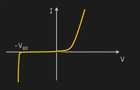
However I can't figure out why the current is creating this "S" shape and why the current form a knee just after the saturation region. The only thing that comes in my mind is the graph of the VI characteristic of a generic PN-junction:

enter image description here

However this doesn't fit well with the formula when I try to see the V in the graph as \$V_{BC}\$.

What am I missing ? Is there a formula to explain this shape of the VI characteristic of the NPN transistor ?
Bemipefe
  • 107
  • 9
  • 1
    [Here is the first level Ebers-Moll equations (EM 1)](https://electronics.stackexchange.com/a/252199/38098) describing the BJT behavior. This ignores bulk impedance at each pin and charge storage (EM 2), and basewidth modulation (EM 3.) But it is very simple and a relatively complete non-linear DC model when considered at a single operating temperature. Does any of that help you? Or do your questions still stand? Some useful charts are [here](https://electronics.stackexchange.com/a/438889/38098), too. Particularly, see Figure 2.17 there. – jonk Nov 12 '20 at 00:23
  • [Here](https://electronics.stackexchange.com/a/357987/38098) is some added information about some reasons why beta varies as it does even in the forward active region. With really high currents the bulk impedance presents significant voltage drops, as well as the current crowding issues. If interested in many of these details, as well as references to all of the important papers, you could do little better than find and buy Ian Getreu's "Modeling the Bipolar Transistor." I helped him get it republished, recently. But I receive no monetary benefit. Only the satisfaction in seeing it being read. – jonk Nov 12 '20 at 00:32
  • draw the diode characteristic highlighting the reverse saturation current. A transistor is basically a diode where you can modulate the saturation current by injecting carriers. The knee in the NPN chars is the 'knee' in the origin of the diode chars. Do not be misled by the breakdown at Vbd, that one is not shown in your BJT chars. – Sredni Vashtar Nov 12 '20 at 00:53
  • Thanks @jonk there is world behind that curves. I knew that the non-linear component world was more complex but who could imagine that such amount of quantum physics and models would be behind the scene. I don't think I will ever model a BJT but is good to know that there an appropriate book for this. – Bemipefe Nov 13 '20 at 09:41
  • @jonk I think that the Ebers-Moll equations (EM1) are enough for me. From these equations I can see that the current is heavily dependent on the temperature. The collector current \$I_C\$ is a sum of exponential functions and these functions just express the static characteristic of the two PN junction (last image in my post). So \$I_C\$ is also an exponential and this explain to me at least the central part of the curve but it's not straightforward to me to see the "knees" in the graph. What does the "intersection" circuital symbol represent ? Parasitic resistance in the PN-junction ? – Bemipefe Nov 13 '20 at 10:28
  • @SredniVashtar So If I understood correctly you are just saying that the collector current has the same shape of the generic PN-junction characteristic (escluding the break-down voltage part which is not shown in the NPN chart). This would explain to me the NPN chart in the reverse active region and saturation region but what about the forward active region ? Why there is a knee when the current passes from saturation region to forward active region ? Is the PN-junction subjected to this behavior too ? – Bemipefe Nov 13 '20 at 11:57
  • The forward active region of the transistor is equivalent to the reverse characteristic of the diode (the one with the constant reverse saturation current - terminology here does not help in separating things). IIRC, you can find a picture of this on Streetman's semiconductor book. The 'knee' is what you would see if you magnified the characteristic of a diode near the origin for V<0. Formulae for the curves can be found on Millman, see my comment in one of the linked questions. – Sredni Vashtar Nov 13 '20 at 12:50

0 Answers0