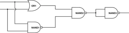
My textbook says that this figure requires twelve pins. Can anyone explain why this combination of gates requires twelve pins?
My textbook says that this figure requires twelve pins. Can anyone explain why this combination of gates requires twelve pins?
Using individual gates, externally connected (so you connect them as you see fit) , 3 per gate + 1 for power + 1 for ground. That's 11 pins. Round up because most dual inline chips (DIP, soic, etc) only come in even numbers. 12 pins, one NC (non-connected). Smaller chips occasionally come in odd number of pins, 5 pin SOT-23 being a good example. You can get single gate ics in sot-23 5 pin.
This is essentially a duplicate of your other question What exactly are pins in the package?.
If you're trying to calculate the "pins required" to do a design, the reason is probably to try to minimize the cost of the design, if it were to be implemented in 1980's-era logic ICs. This calculation is essentially irrelevant to design in the technology you would use for it today, like an FPGA, CPLD or 1- and 2-gate logic.
In discrete logic, you would minimize the cost of this logic by first minimizing the number of packages you buy, then minimizing the number of gates you use within those parts (which reduces cost only if you can actually share these gates with other logic in your design).
To implement this circuit, you have the choice between buying a chip of OR gates (likely 4 gates per chip), a chip of NAND gates, and a chip of AND gates (and wasting all but one gate on each chip), or, implement the AND gate as a cascade of two NANDs, and then just buy a chip of OR gates and a chip of NAND gates.
Since the second choice is more economical, you can actually view G3 as a gate requiring 6 pins --- three for the first NAND gate, and three for a NAND gate wired as an inverter.