5

enter image description here

enter image description here

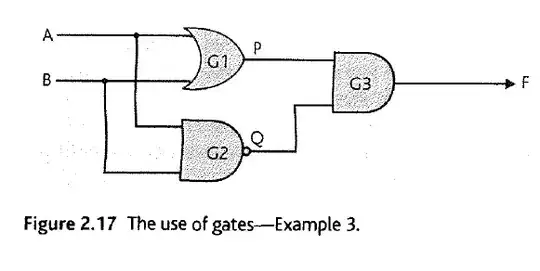
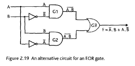
Both describe EOR(XOR) gate - but according to the textbook, it says that Figure 2.17 has two gates in series, while Figure 2.19 has three gates in series. But to my eye, it seems that both have three gates in series! Can anyone explain this? Thanks. Or is textbook's figure somehow wrong? (I heard that the textbook Principles of Computer Hardware has few figure errors in digital logic areas.

user17534
  • 471
  • 2
  • 5
  • 5

2 Answers2

7

You must evaluate the longest path any input must traverse, in terms of gates, in order for the final output's value to be resolved. The textbook is correct in saying that the longest path is two gates in Figure 2.17: Either input has two possible paths, one is G1-G3, the other is G2-G3, therefore the maximum depth (or delay) of 2.

Perhaps you are being misled by the NAND gate G2, which you may be thinking that is composed of an AND and a NOT, therefore being by itself two gates in series. But that is not necessarily true, the NAND can be a single gate by itself. To understand why, it helps to see how it may be constructed in, for example, CMOS technology.

apalopohapa
  • 8,419
  • 2
  • 29
  • 39
1

No, the textbook is right. Remember the difference between resistors in parallel and in series? This is pretty much the same.

The difference between 2.17 and 2.19 is the inverters. Those inverters are an extra step in the gate series, therefore 2.19 has a series of 3 and 2.17 one of 2.

You can see this from the input side of view: in figure 2.17, the input will first go through G1 or G2, and after that G3. That's two steps. G1 and G2 are symmetric, so they are parallel. But since the output of G1 is connected to the input of G3, they are in series.

In figure 2.19 though, the input will be inverted first, so that's en extra step. The inverters are symmetric thus stand parallel, G1 and G2 too, and G3 is alone.