3

I'm trying to understand how can one build a circuit that does the following functionality:

enter image description here

I see according to the output that I should have a D-FF, that works at Falling-Edge mode, so I need to add an inverter to the CLK. how can I continue from here? are there basic rules that I can follow in order to know what should I add more?

Note: my intention is to use D-FF in the circuit. I have knowledge in designing mealy machines and aware of the procedure. but here the states aren't quiet clear in order to make mealy machine design. I would like to know if this could be a successful approach for the problem. the reason I thought about mealy machine is because the output change is dependent of the input change.

Firas Abd El Gani
  • 1,021
  • 7
  • 15
  • The diagram is not clear enough. When the first transition is happening? When the rising transition of the second output plus is happening? – Eugene Sh. Oct 28 '20 at 15:30
  • I modified the diagram. thanks for the note. – Firas Abd El Gani Oct 28 '20 at 15:45
  • Why do you need to do this? There are pitfalls, particularly with the setup time to the clock edge. You might miss the rising edge of IN altogether. Or you may end up with an OUT pulse too small for whatever it's going into to recognise it. – Finbarr Oct 28 '20 at 15:49
  • You can certainly do this with a flip-flop and a logic gate, but this smells to much like homework. Why don't you tell us about the bigger picture? – Elliot Alderson Oct 28 '20 at 20:06
  • @Andyaka Yes, I just picked the best answer. Thanks for reminding me. – Firas Abd El Gani Nov 29 '20 at 12:35

3 Answers3

4

You could consider starting down the route of an edge detector using an EXOR gate: -

enter image description here

That gives you a kick in the right direction by producing a pulsed output each time IN changes state. If you need to extend the pulse, use a monostable or, if it should extend only as far as the next positive going CLOCK edge then use a D type flip flop to latch the pulse and clear it on the rising clock edge.

Picture also available in this answer.

Andy aka
  • 434,556
  • 28
  • 351
  • 777
3

An edge detector like this should do the trick: dual edge detector

enter image description here

If the output falling edge needs to be synchronized with the rising edge of the clock, then feed the pulse output into the clock input of a D-Flop and the input clock to the reset input of the D-Flop. D input is tied high. The example circuit assumes the D-Flop uses low for reset. If high for reset type, then NOT3 gate can be removed.

schematic

simulate this circuit – Schematic created using CircuitLab

Aaron
  • 7,274
  • 16
  • 30
  • This circuit only has a single input, where OP asked for a circuit that makes a 0-1 transition in response to one input and a 1-0 transition in response to a second input. – The Photon Oct 28 '20 at 16:15
  • @ThePhoton Trace `A` and trace `Edge pulse` match the OP trace `In` and trace `Out` respectively. I don't see what you are referring to with the 1-0 transition for a second input. – Aaron Oct 28 '20 at 17:02
  • OP said the output should go low when the CLK input goes high. Your circuit does not have a CLK input. – The Photon Oct 28 '20 at 17:15
  • @ThePhoton I don't see that in the OP. Maybe it was removed during one of their edits? – Aaron Oct 28 '20 at 17:18
  • It's in the title of the post: " high output between input transition and **next rising edge of CLK**" – The Photon Oct 28 '20 at 17:19
  • Maybe there is some interpretation there. "high output **between** input transition and next rising edge of CLK." As long as the clock speed is not on the order of the propagation delays, this will happen reliably. – Aaron Oct 28 '20 at 17:34
  • Their timing diagram shows the pulse ending when the clock rising edge arrives. – The Photon Oct 28 '20 at 17:35
  • @ThePhoton Updated answer to make the solution comply with the timing diagram explicitly. – Aaron Oct 28 '20 at 17:43
  • @Aaron, thanks for the solution. it really does what I intend to do. – Firas Abd El Gani Oct 29 '20 at 06:18
  • @Aaron you added an XNOR in the solution but actually meant XOR? – Firas Abd El Gani Oct 29 '20 at 06:27
  • @Xhero39 You are correct. I updated the drawing. – Aaron Oct 29 '20 at 16:22
2

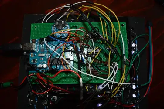
You're delving into the realm of asynchronous state machines, a tricky but very interesting part of digital logic design. Essentially you need some basic combinatorial logic combined with some asynchronous feedback. If you look at the internal structure of a flip flop (at least the historical method of construction) it's essentially some cross-connected NAND gates with feedback.

The text I used as a reference is by David J. Comer, "Digital Logic and State Machine Design". In the last chapter or two, asynchronous design is covered in detail.

Your waveforms don't specify every possible transition case, so I made a few assumptions about what you want, then came up with this state feedback table, reduced expressions, and a circuit that implements it without any explicit flip-flops.

Asynchronous Circuit Design

The state table (might need adjustment to change my assumptions):

enter image description here

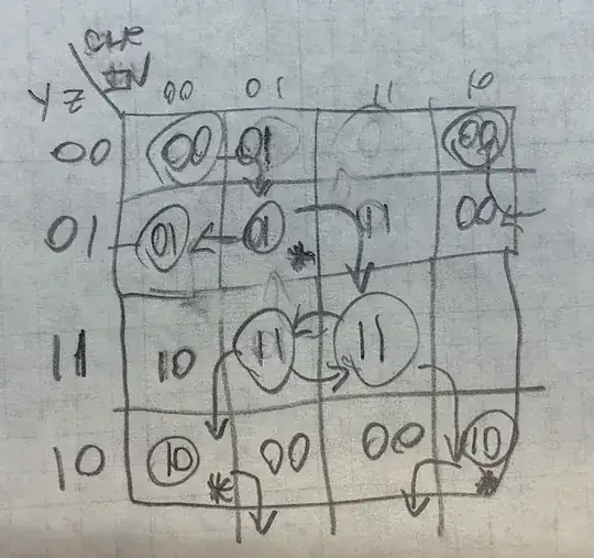
When the value in the cell of the Karnaugh map matches the value on the left side of the table, you are in a "stable state". An asterisk (*) in the table indicates that the output signal should be high in that state. When the value inside the table is different than the value at the left side of the same row, the state is unstable and the state machine will change to the row number indicated inside the state cell. For example, when both signals are low, we start in the top left corner (and YZ also equals 00). When the "IN" signal goes high, we move one cell to the right in the Karnaugh map, where the value of "01" takes us to the second row (where YZ are "01"). Since that cell also contains "01," the state is stable. The asterisk in that cell indicates that the output should be high, and so on.

Apologies for any small errors, I didn't have a chance to simulate the full circuit, but the general approach is valid.

It's this kind of complexity that typically drives us to do fully synchronous design, because it's easier to design and analyze.