6

Objective

I want to design a tiny single packaged mains-powered temperature sensor. Possibly as a multi-chip module (MCM) on one small PCB board.

Constraints

The temperature sensor I plan to incorporate:

  1. Operates (Iq) between 1VDC, 10mA and 3VDC, 30mA
  2. It is a 65nm Samgsung fabraction process. So it is very small.

Power source:

  1. around 220V mains powered (single-phase)

  2. Operation without a secondary source (batt, bulk cap, et. al.) desired to minimize size.

  3. The efficiency demanding is just >10% and that is enough for me.

Ideas now

I was intended to design my power converter into a small chip, thanks alot for people's suggestions . I think about charge pump, and different IC modules, the RF powerharvesting, and the possibility for implementing such a device on nm Si process. Above all, microchips that can convert 220V ac to low dc is big-size for me, and also have lots big caps around module; charge pump from Olin's idea, I dont think I can design diode that can support high-voltage on chip, if not on chip, it will be big size(I think); for powerharvesting, I did some research before, and honestly it is good, but RF energy is not very solid, and there are some limitations about the distance. So I go back to the original ideas how to convert voltage. Hope your guys can check if they are right. I will use some regulating stuff(off chip) to regulate the voltage at last, so i just wanna check if the thoughts are right.

1> Linear with the resistors. Input 220Vac to the two resistors,one is 1Mohm, the other is around 10Kohm,figure below:

enter image description here

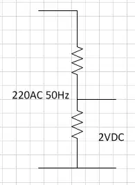
I know the efficiency is verylow, about 1%, so I drop it. But it is my earliest idea.

2> linear with the capacitor. Since the first way efficiency is so low, I wonder can I use two capacitors to replace the resistors, (figures below) one cap is 1pf, the other is 10fF (the exact values are not certain).

enter image description here

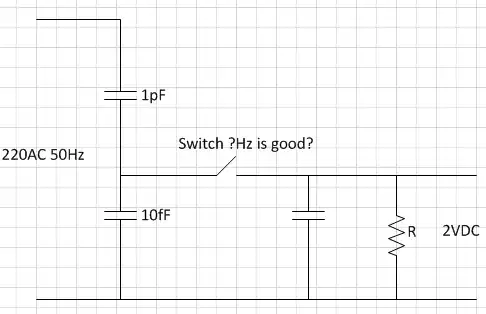
also I wanna design the big capacitor on my pcb board by myself like figure below,so I can mini-size. If the cap value is not big, I can design it on chip.

enter image description here

First I dont know if the fundamental of circuit (the first figure) will work or not, because I never see this before, but as I know, I hope it works. Assume it works, how to design it exactly ( I mean how to design the cap value properly and how to choose the switch frequency properly).

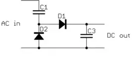
3> The conventional linear isolating converter:

enter image description here

My question is, in this conventional way, the output current in other designs usually needs big, so the transformer is big, but I just need it very small(1mA~30mA), so according to your view, how big it will be, I know little about transformer design. the voltage ratio is 45:1, and the current is 1:45, how many coils on both sides are good ? How big it will.

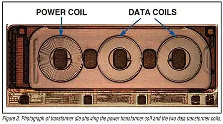
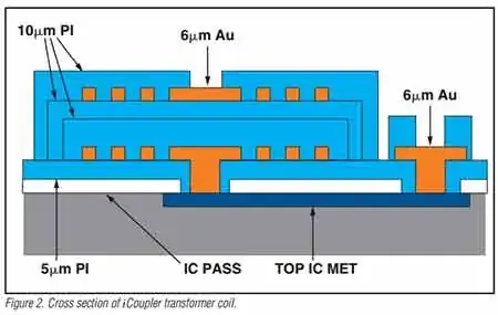
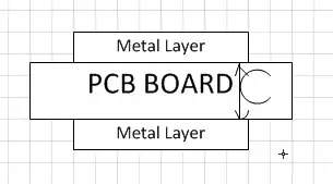
if the transformer above is not so big, Furthermore, my design method for the transformer is improved, and I wanna design transformer on PCB board by myself, like figures below:

enter image description here

in my first figure, I just use one stage transformer, if size is big to design 220V-5V converting, maybe I can design two or more stages to convert like 220V-48V-5V. I hope the transformer (each stage, hope one stage is enough) is less than 1cm×1cm. If that is possible, I WILL do it. And I think the efficiency is good, and also safe.

Above all, I want to improve my design in the No 2 and No 3 method, but I dont know if my thoughts are right or not. Ready to get judgement now.

alan
  • 787
  • 2
  • 7
  • 15
  • 3
    We *STILL* don't know whether this power supply needs to be isolated. That must be decided first since the solutions either way will be very different. You say this will power a sensor, but where does the output of the sensor go? You also ask about a connector, so it implies the sensor signal may go elsewhere. If the sensor signal is just to be displayed locally, for example, then the supply could be isolated, but then the question about connector makes no sense. Also, what is this about, the electronics or the connector. Pick one. – Olin Lathrop Jan 02 '13 at 14:16
  • If the "connector" is just to plug into the wall outlet, then I don't see what the problem is. Use whatever the standard wall plug is for wherever this device will be used. As for 220 VAC on a chip, not gonna happen. The supply needs to be external to the chip, then whatever chips you have run from the resulting low voltage DC. A charge pump may be suitable, as I suggested to your original question days ago. – Olin Lathrop Jan 02 '13 at 15:33
  • Charge pumps can certainly step down as well as up. At high step down ratios, they look more like current sources. The current is a function of the capacitances and the pumping voltage and frequency. Capacitive charge pumps are common in un-isolated supplies that only need to put out a few mA. They are also fairly efficient. You would likely need to add some sort of regulation afterwards. This can be as simple as a zener shunt regulator since from 220V to 3V the charge pump will look like a current source. – Olin Lathrop Jan 02 '13 at 17:12
  • @OlinLathrop I edit my question again, and thinks different methods for some time, hope you can check – alan Jan 07 '13 at 01:06
  • you should be made aware of this new answer to a similar sort of question here http://electronics.stackexchange.com/questions/53587/cellphone-charger-has-no-transformer#53628 – placeholder Jan 10 '13 at 17:32
  • Chip designing is totally out of my profession. 1V 10mA consumption equals to 10mW dissipation. If you make ANY type of regulator with 10% of effieciency you will end up at 90mW PSU + 10mW sensor dissipation. Isn't that too much? I mean, this will be a single-chip temperature sensor, won't that dissipation affect the measurement significantly? – Gábor Móczik Aug 11 '16 at 22:31

7 Answers7

8

What you are looking for is called an off-line power supply. A quick search reveals the Fairchild Semi FSAR001. Putting in 80 - 240 Vac yields 5Vdc at 35 mA max.

There are many more around.

  • it is NON-isolated!!! meaning this is not a design to put into devices that people will handle - Full Stop.

let me repeat that, this is a lethal circuit, but perfectly reasonable to use under the right conditions.

Here is a snip from page 2 of the datasheet. enter image description here

This answer does not address your question concerning a chip design. Which I can answer but I'm hoping that the real problem is solved with this lead and direction.

placeholder
  • 29,982
  • 10
  • 63
  • 110
  • +1 Nice work. I didn't consider the non-isolated case... – DrFriedParts Dec 31 '12 at 05:10
  • Nice answer! But what about the efficiency ? I cant find it, such non-isolated line regulator, I think the efficiency will be less than 10%. Welcome to correct~ – alan Dec 31 '12 at 05:57
  • It might be very low, there are types of these that use capacitors as the coupling element, which in turn makes it more efficient at the expense of more reactive power (and poorer power factor) – placeholder Dec 31 '12 at 06:32
  • Again, how can I find such coupling capacitor type product? what should I google, also do you know what is the max efficiency this type it could be? If the efficiency is 30%-50%, I am happy to use it. BTW, have you considered to build the SMPS type into a chip? is it possible to do? I can put the big capacitor outside the chip, and for the rest, is it possilbe to on chip? – alan Dec 31 '12 at 06:54
  • The datasheet does not give a method of calculating the power. However the technique used is to charge the cap through a conduction angle and use a LDO to run off of that. I would have thought a bridge rectifier on chip would have been better (parts like that I've used in the past). But a cursory examination shows that it can't be TOO bad. 200V @ 35 mA = ~ 7 W, which a DIP package CANNOT handle. I'd say it would have to be 90% + efficiency or better because of that fact. – placeholder Dec 31 '12 at 06:56
  • You mean this FSAR001 efficiency is 90%+ ? or the coupling capacitor type ? This FSR001 circuit is DIP package. I am a little bit confused. Also, when you say " which I can answer but ...." you mean you designed such AC/DC chip before? what kind of structure is the best in your view ? Have you tried the SMPS structure? Just asking.. – alan Dec 31 '12 at 07:13
  • @alan - The FSAR001 efficiency will be high when considering efficincy as (Vin x Iin) / (Vout x Iout) . BUT it's power factor is ppor - which often does not matter. It works by turning on a switch when Vin_mains is low and turning it off when Vin_mains >> Vout. If your IC process can withstand mains peak voltage you can build it into your IC. If not then you can add it using one high voltage switch (bipolar transistor etc) plus a low voltage IC. This is a very clever circuit and also easily unreliable if designed badly. It will do what you want if designed well. – Russell McMahon Dec 31 '12 at 13:11
  • @rawbrawb this circuity around the IC001 needs some very big capacitors, it is not what I really need. If my power efficiency demanding is just >10%, and I wanna design it to a chip, do you have some experience doing this or some suggestions? – alan Jan 02 '13 at 12:43
  • Answered as a separate answer. Because I believe that the chip design side is extraneous and the question should have been posed as two parts. One is, how to do this with minimal parts?, and two, can it be designed as a chip? – placeholder Jan 02 '13 at 18:48
  • yes, you are right. and you answer is certainly to my first one, ^_^. Thanks anyway – alan Jan 03 '13 at 00:58
  • @rawbrawb I edit my questions again, and think about the nm Si process implementation possibility, and still think I can just chip the 5Vdc-1Vdc something like this, for 220V-1V, it is very huge, and I have some original thoughts for this, hope you can check the edited ones. – alan Jan 07 '13 at 01:08
6

No getting around physics. You will need a "wall wart". Either you get a wall wart as a packaged product or you implement it yourself on your PCB.

Here's why your ask isn't feasible:

A wall-wart...

  • performs rectification (converting bi-polar AC power to uni-polar AC power)
  • followed by filtration (converting uni-polar AC to an approximation of DC)

Those are the basic steps to get from AC to DC. Any alternate approach will include those steps in some form. You can get much smaller (lower output power) units if that would suit your needs better. You can also get them as PCB modules (google for "open-frame" power supply) instead of packaged products.

For example, these.

DrFriedParts
  • 12,482
  • 36
  • 54
  • if I implement the wall wart on my PCB, what it will look like, is there any pics I can see? I mean if I can design most of the components into a 65nm CMOS level components in a chip, so I can make it much smaller, right? for example, I can design the onchip transformer, and it is not big at all. – alan Dec 31 '12 at 02:57
  • Huh? Your a chip designer? In any case, no. To the first order, you won't have enough isolation that way. It won't be safe. Look at those products I linked to above. Those are examples of small packaged solutions. – DrFriedParts Dec 31 '12 at 03:16
  • you mean, converting the bi-polar AC to uni-polar AC by the diode bridge is the first order? Yes, I am a chip designer, so I am not sure if I can design the converter into a chip or not. I checked the web you told me. I saw the Open frame PSU, it is not what I want, there are very large components, and I hope I can design the diode bridge, and the inductor, and some of the capacitor(maybe some are to big, so I need to put outside), and the transformer( the transformer is not very big on the pcb, I think I can change the Fe-winding transformer into a on chip stack-twisting transformer)onchip – alan Dec 31 '12 at 03:33
  • Perhaps that level of detail should go in your original question. I would suggest that you change the title to "Is an on-die 220V capable SMPS possible?". That would attract more of the semiconductor-focused part of the community. As far as I can estimate in my head, at 220V you would not be able to maintain enough isolation in 65nm Si. – DrFriedParts Dec 31 '12 at 03:38
  • Can I put the diode bridge and the flitering capacitor first outside the chip, and just design the high DC-low DC part into a chip? Do you think it is possible? Is there any high DC-low DC converter chip in the world now ? – alan Dec 31 '12 at 04:16
  • Yes and yes. Many many. But that isn't efficient (FYI). – DrFriedParts Dec 31 '12 at 05:12
  • This answer is severely incorrect. Until quite recently, hardly any "Wall warts" were switch mode. The developing trend of making them that way has been great, but it's quite ignorant to claim that a wall wart is necessarily switch mode when there is a huge installed base of linear units, and more still being made. – Chris Stratton Dec 31 '12 at 16:24
  • @Chris -- Yes, agreed. actually, that was an error on my part. I didn't mean to have three bullets. I was writing something else and then decided to switch approaches to the more general statement about rect + filt. Somehow I missed that I still had my original bullet there. Corrected with apologies. – DrFriedParts Dec 31 '12 at 19:26
  • Many problems with this answer. (1) The on-board and off-line switchers refute the "must be a wall wart" statement. (2) If it's on a board and not on the wall, it's not a wall wart. (3) Some output AC, others DC, still others, regulated DC. The one thing they have in common, you left out: (4) They all provide isolation! This is practically the reason wall warts were invented! – gbarry Jan 02 '13 at 18:03
  • @gbarry -- fair points all... that said, in the context of the original OP's question (which has been heavily revised) he defined the term to effectively mean "a device that plugs into the wall and converts AC-DC," hence my answer saying that basically, you can't convert AC to DC without a device that converts AC to DC... not exactly my most profound answer on SE ;-) – DrFriedParts Jan 02 '13 at 22:39
  • @DrFriedParts I edit my questions again, and change something I want to say, I think about your suggestions, and go back to the original thoughts, hope you can check it. – alan Jan 07 '13 at 01:11
5

The FSAR001 circuit suggested by rawbrawb is a clever one that will do what you want better than almost any other circuit IF designed well. But it can be very unreliable if badly designed. This is because transients or unintended signals can turn on the input-to-output switch when it should not be one. Mains is then connected to output directly. This is usually 'a bad idea' [tm].

The FSAR001 circuit efficiency will be high when considering efficiency as
(Vin x Iin) / (Vout x Iout) . BUT it's power factor is poor - which often does not matter. ie it draws all its power when the mains cycle is at low voltage and none at all when voltage is high so the waveform is VERY distorted compared to a sinusoid. Regulatory authorities are increasingly unhappy with such systems BUT when power levels are very low (as here) it may be considered acceptable.

It works by turning on a switch when Vin_mains is low and ~- Vout, and turning it off when Vin_mains >> Vout. If your IC process can withstand mains peak voltage you can build it into your IC. If not then you can add it using one high voltage switch (bipolar transistor etc) plus a low voltage IC. This is a very clever circuit and also easily unreliable if designed badly. It will do what you want if designed well.

A design which can be small and which is potentially safer is to rectify mains and then to use a very high frequency oscillator to transfer energy via a magnetic core. The higher the frequency the smaller the core. Some modern converters operate in the 1 MhZ - 10 Mhz range to get size low. Even higher frequencies are possible with due care.

A recent approach is to generate RF at extremely high frequencies - 1 GHz + in some cases, and to use very very small capacitors as energy coupling devices. This can result in extremely small systems but complexity is higher.


Korea? A visit there would be interesting ... :-).

Russell McMahon
  • 147,325
  • 18
  • 210
  • 386
  • Thanks very much for your answer, I am very interested in the last method---"generate RF at extremely high frequecies, and use very small capacitors..." Can this methold be used to design the high efficiency AC/DC converter? Can you give me some links or websites about this coupling capacitor system design? Thanks – alan Dec 31 '12 at 19:10
  • @RussellMcMahon Korea sounds interesting indeed. For a reasonable fee, a much-needed professional help can be obtained. – Nick Alexeev Dec 31 '12 at 22:03
  • @alan - This is not exactly what I meant but will give you some ideas. http://www.powercastco.com/PDF/P2110CSR-SL-UsersGuide.pdf This transfers power from a 915 MHz source. It does not use capacitive coupling but may give you some ideas. I had a quick look with Google and found the above. Sleep calls here, but if you search on eg RF Power transfer capacitive - or similar - you should find useful links. – Russell McMahon Jan 01 '13 at 15:00
  • @alan - Here's another - closer to what you want. https://www.google.co.nz/url?sa=t&rct=j&q=&esrc=s&source=web&cd=14&cad=rja&ved=0CEgQFjADOAo&url=http%3A%2F%2Fciteseerx.ist.psu.edu%2Fviewdoc%2Fdownload%3Fdoi%3D10.1.1.126.5786%26rep%3Drep1%26type%3Dpdf&ei=0f3iULycFqbsiAfUzYCABg&usg=AFQjCNF_mv1IoRh1Ae1_1aGWrHRCaTGsfA&sig2=SHXNAkejecjN5gTaWFPrEg&bvm=bv.1355534169,d.dGY – Russell McMahon Jan 01 '13 at 15:17
  • @RussellMcMahon thanks, I checked this paper, and the effective distance is not very long, it could not be 10 meters forever, maybe. It is not what I really need. Also the FSR001 cirucit is not what I need, the appliation diagram capacitor is so big, and i just need very small things, and if I want my efficiency is just ≥ 10%, and that is enough, and output is 1V, about 30mA. Do you have some suggestions about how to design this circuit into a single chip? – alan Jan 02 '13 at 12:36
  • @Alan Saying "this paper" is not helpful. Which paper please? - I referenced several. "POwerharvester" offer a number of solutions. See http://www.powercastco.com/products/powerharvester-receivers/ and http://www.powercastco.com/PDF/Powerharvester-Brochure.pdf - You can work over mm range. You do not have to use many meters range. // Did you look at my second reference which is an ON-IC system? – Russell McMahon Jan 03 '13 at 15:42
  • @RussellMcMahon I am thinking it... I will organise my thoughts on weekends, and edit my question again. Thanks a lot. – alan Jan 04 '13 at 12:13
  • @RussellMcMahon honestly, the RF power harvesting is a good choice for me, I did some research on this before, and I think it is a method to realize what I want, and thanks a lot. But there are some limitations about the distance, and the RF energy is not very solid, so I hope, if I really cant do my way, then I will think about this one. I edit my questions again, and go back to the very original thoughts, hope you can check it. – alan Jan 07 '13 at 01:14
  • @alan - I do not know what your knowledge level is but you seem to not understand quite basic electronic concepts. It would help people if you explained what level you are working at - is this an assignment or a project and what is your knowledge level. || For capacitor transfer at mains frequencies the capacitor is such that Vmain / Xcap ~~= Current required. Xcap ~= 1/(2. x Pi x frequency x Capacitance) so you can calculate capacitor values. The ones you suggest are far far far far too small. – Russell McMahon Jan 08 '13 at 07:43
  • @alan - || If using a transformer at mains frequency then the impedance of the input winding at mains frequency has to be high enough to cause "magnetiation" or idle current to be small wrt load current. Your single layer PCB windings are far far far far too small. You can use coils about the size you suggest using the system described by Anindo Ghosh. Do look at [the application note he mentioned](http://www.analog.com/static/imported-files/overviews/isoPower.pdf) and the related [ADuM524x data sheet here](http://www.analog.com/static/imported-files/data_sheets/ADUM5240_5241_5242.pdf). – Russell McMahon Jan 08 '13 at 07:47
  • @alan - The ADuM524x ICs tend to transfer about 5V at 10mAusing a 300 MHz signal. You could use your own system to transfer power at whatever level you wished. || Their system is low voltage to low voltage BUT you could make a 300 mHz (or other) oscillator that was mains powered and a low voltage output. – Russell McMahon Jan 08 '13 at 08:00
  • @RussellMcMahon about the linear capacitors, I know what you mean. The cap I suggested is small, but I can change it into the magnitude of nF, I make the cap is 120nF and 12uF, and the load is about 1Kohm, the result I can get is about the 2V, and 2mA AC, then, I plan to use a chip to convert this to what I need. I am sure it works and I simulate it on cadence, and also the capacitor doesnot consume power, so I will use my chip to replace the load, and I am thinking, it is possible to realize it. What is wrong with that? BTW, I cut off the switch in my simulating circuit. – alan Jan 09 '13 at 07:06
  • @RussellMcMahon about the linear capacitor method, since capacitor does not consume power, and also can divide voltage, assume my required current is 10mA, and U x W x C = I, C~~= 10mA/(220 x 2 x Pi x 50 )~~= 140nF, I use 120nF and 12uF, and 1kohm parallel with 12uF, it is working in my circuit. my only issue is that, you think hard to build a 12uF and 120nF capacitor on a PCB board? – alan Jan 09 '13 at 07:16
  • About the main transformer method, I also think it is too big to build it. and I am reading that paper, and if my linear capacitor method is working, and the efficiency is enough( since the cap consume little power, I think the efficiency is enough ), I will drop it, but I have to say, that paper is very good, and since Anindo Ghosh posted, I am reading it,and doing research about that. – alan Jan 09 '13 at 07:20
  • "You could use your own system to transfer power at whatever level you wished. || Their system is low voltage to low voltage BUT you could make a 300 mHz (or other) oscillator that was mains powered and a low voltage output" I dont understand it. I know this device is low dc to low dc, which btw, I can design low dc to low dc in a nm process chip by myself. I only find the transformer is intersting. Even I can design a oscillator powered by main line, I still need a low input voltage for this device to get anohter low output voltage, which is absurd, cause what I need is a powersupply. – alan Jan 10 '13 at 03:36
5

Now to answer the "chip design" side of the question. This answer cannot by necessity cover all the details. You'll have research individual areas your self, which I hope to provide leads to in the text.

The first step you'll need to do is to find a process that can handle the high voltages that are required.There are limits to the materials that are used here that scale with electric field strength. There are Si processes that span from 1000V down to 1 V so we'll assume you'll find a Si process (Bipolar, BiCMOS or CMOS) that can handle the voltage.

You seem fixated on 65 nm process technology. Doing a rough calculation and assuming 1V operation, to scale this design to handle 600 V you'd need a 39,000 nm process node = 39um. And that is to support the lateral e-field from Source to Drain. That in it self is a big hint that this process wouldn't be used. In fact higher voltage process nodes use slightly different devices, like DMOS. The offline controller chip is most likely made in a 1 or a 2 or a 3 um process, and may actually be SOI.

The highest voltage, smallest process node I am aware of is ~ 50V on 0.18u CMOS process, - automotive qualified. There could be others out there. Look around. Since you are in Korea look at Magnachip and Dongbu Hightech. as fabs.

Assuming you've now picked a process that can handle the voltage and the 65 nm process node is long gone from your thoughts. You are now a hero because the NRE for the process has gone from $1M (65 nm node) to maybe $60K (3u node).

So can we put inductors on chip? Absolutely. but they are HUGE, and very hard to make in a way that has good yield. RF guys use them for Tank circuits and filters. But the thing to remember is that the inductor sizes used in RF circuits are about 1/1,000,000 the inductance that you will need to do a good SMPS convertor. And NO you can't put a high permittvity material down to boost inductance, you are stuck with SiO2 and it's various variations. So POWER inductors are out of the equation now too.

Next, capacitors. Based upon a known process node - 180 nm, supports 1.8 Volts and has 8.8 fF per um^2 capacitance. Lets scale this to 600 V by increasing gate oxide thickness. => 60um thick gate oxide to prevent rupture. (E-field stays the same). Capacitance is 1/333 => 26.4 aF/um^2. For 10 uF you need 3.8e11 square um to get that capacitance. => 0.4 m^2 notice that is a die that is roughly 0.6 m X 0.6m on a side. I think that cost starts to become an issue then. That offchip capacitor now starts to look very reasonable.

Now all the design constraints are in place. Using an old, high voltage process node, with no access to on chip inductors or capacitors. But it's inexpensive! And you get proper analog transistors vs. the digital ones you'd get in the 65nm process.

The only solution I can think off, since you can't use any capacitors off chip, is to build a full wave rectifier and ONLY operate the circuit when the the input voltage is above the 3 V threshold of operation. Have the circuit shutdown during the AC waveform zero crossing. That way you don't need the "big" hold capacitors. Once the AC waveform is above the 3V range around zero crossing you'll have plenty of power. You could put much smaller filtering, charge holding capacitors on the bias circuits (that don't consume much power) to allow the operating point of the circuit to stay fixed during the varying power supply. And you can reduce power. You should be able to get a good bandgap circuit that operates on less than 1 uA so that means far smaller capacitors. But it means that you can only communicate during the AC voltage "high" phase.

placeholder
  • 29,982
  • 10
  • 63
  • 110
  • Thanks for your answer, and I think about your suggestions a lot for this weekend, and i edit my question again later, thanks – alan Jan 06 '13 at 14:18
3

Isolated power step-down and rectification from mains power line, as well as power, analog and digital blocks on a single die are possible, and are being done by at least a couple of manufacturers, Analog Devices being noteworthy in this regard.

Transformer on a Chip

Analog Devices isoPower iCoupler devices achieve 5 kV of isolation, with single-power-source operation, through their in-chip microtransformer technology. While their current isoPower portfolio does not apparently offer any microcontroller or temperature sensor devices, the technology concept proof should serve to point a chip designer in the right direction.

The paper referenced above provides detail on isolation geometries, gaps and materials parameters for their designs.

iCoupler Transformer cross-section

Some salient points from the paper:

  • The microtransformers are built on a CMOS substrate, and a 20 µm thick polyimide layer in between the primary and the secondary provides HV isolation up to 5 kV.
  • Rectification of the secondary is achieved through integrated Schottky diodes
  • A linear regulator on the secondary regulates output power, thus allowing the devices to output regulated power to supply additional logic-level components.

In short, the isoPower line is almost an ideal match for the power aspect of the requirements stated in the question.

Once single-chip isolated regulated power is achieved, the temperature sensing and display functionality can be addressed as a more conventional chip design / MEMS problem.

Anindo Ghosh
  • 50,188
  • 8
  • 103
  • 200
  • I am reading this paper now, and I think it is really good. BTW, how do you think the linear capacitor method to drop the voltage to what I want, I simulate my circuit, and using a 120nF and 12uF capacitors, and a 1Kohm resistor parallel to 12uF capacitor, the output of the resitor is almost 2V AC, I can adjust some values after designing the sensor chip, do u think there is a problem for that? I doubt a lot for that, I wanna build the cap on pcb board by myself(double sides'mental on pcb can be as a cap), but I need to find out is this a way to go? I dont see anyone did this. – alan Jan 09 '13 at 12:16
  • No, using double-sided plating on a PCB will not give consistent capacitance, nor will it give high enough capacitance for any useful purpose. The capacitance between two charge planes falls drastically with distance between the planes... PCBs are just way too thick. Also, this probably merits a separate question. – Anindo Ghosh Jan 09 '13 at 12:19
  • I have some questions about that paper, the transformer design is really impressive, but the drive frequency is MHz, and the main line frequency is just 50Hz. Also, The device is a DC-DC converter, low input DC to low input DC, which I can design by myself with a nm process chip. The only thing I find is very interesting is the transformer, but I am not sure how to use it with the 220V AC main line. It seems that I cant just use this transformer to connect the AC main line, and get a low voltage AC. – alan Jan 10 '13 at 03:20
  • @alan The tech response folks at Analog Devices may be able to provide insights into the paper as well as more recent enhancements in isoPower. They have a fairly active forum. – Anindo Ghosh Jan 10 '13 at 03:36
2

Essentially - no. You will find a very few off-line power supplies on silicon - but they are formed on non-standard processes tuned specifically for high voltage transistors, and not suitable for microcontrollers or general analog circuits. As a chip designer you will not have access to these processes unless you talk to a specialist manufacturer - International Rectifier, Ixys etc.

If you can design your whole system - including sensor - so that it can be completely isolated from access by a consumer - "double-insulated" - then you can probably use a non-isolated off-line power supply like the Fairchild part mentioned above. Then you can devote perhaps a square inch of PCB space to the offline PSU - your sensor and its electronics might live on the same board.

But a temperature sensor, isolated from the environment as it must be for safety reasons, and physically close to a warm-running power supply, sounds fairly useless to me...

This is the reason for the persistent questions about exactly what your sensors are and we still don't have the information from you to answer your question properly.

  • A decent design is unlikely to experience problematic self heating, given the miniscule (if far too vague) power levels imagined. – Chris Stratton Dec 31 '12 at 16:26
  • ...depends on his sensitivity/selectivity requirements. Like you said, far too vague to know for certain. – DrFriedParts Dec 31 '12 at 20:59
  • @Chris - I may have been a *little* harsh - if the OP has given suitable thought to thermal, airflow and safety isolation compromises he *might* come up with what you will allow is a "decent design". But he won't without thinking about them. –  Dec 31 '12 at 23:12
1

You are simply not going to put a line-powered power supply on a chip. The voltages are too high to allow for a reasonable size, and you need other components that require enough energy storage to make them impossible.

I assume this can be a isolated supply since you are apparently trying to build a stand-alone unit that does not electrically connect to the outside world except to the power line. In that case, I still think a charge pump is your best option. Yes, it will be external to the chip, and compared to a chip it will be huge. That's the way it is.

Here is a basic charge pump:

When the top AC input goes negative with respect to the bottom, C1 is charged up to negative the peak line voltage thru D2. As the voltage swings back to positive, it is discharged thru D1 and charges up C3 somewhat. With no load, the DC output voltage is the peak line voltage, which is not what you want. However, the current is well limited, so the simplest thing would be to follow this with a shunt regulator. That will dip between peaks, so you either design the reset of the circuit to tolerate that, or you make the shunt regulator a little higher than what you want and follow that by a normal linear regulator.

One drawback to this approach is that the current you get is depressingly low for nice size capacitors at line frequency. You can make smaller capacitors allow more current, but you'd have to then rectify the AC line and chop it yourself with active circuitry.

There is no free lunch as you seem to be wishing. If what you are asking for was reasonbly possible, others would have done it long ago.

Olin Lathrop
  • 310,974
  • 36
  • 428
  • 915
  • Yes, I know, if what I am asking for was reasonbly possible, someone may do it ago... but I dont know why it is not reasonbly possible.... can you point why my No 2 method is not possible, I can built the capacitors outside chip on my pcb board, and I think from what I have learnt, it works, two cascade caps can divide the voltage, so I can get the 2VAC, then, I will build the 2VAC-1VDC on chip, why it doesnot work? – alan Jan 07 '13 at 06:19