0

This is my first time fabricating a simple PCB. Could you help check for any mistakes in my PCB layout and routing?

enter image description here

enter image description here

  • The power line is 20-25mil. Does the width of the power line vary with the specific magnitude of current or just make it as wide as possible?
  • Due to little component, is it necessary to make lines except power wider?
  • Are there other mistakes in layout and routing?

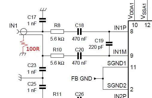
Update PCB with labels.
enter image description here

JRE
  • 67,678
  • 8
  • 104
  • 179
user7476499
  • 153
  • 1
  • 5
  • 1
    Have you run any checks in your layout tool? What checks? What limits does the checker use? – Andy aka Sep 22 '20 at 09:07
  • 1
    Please draw your decoupling capacitors next to their respective IC. How come you are not using a ground plane? – winny Sep 22 '20 at 09:38
  • 1
    I have drawn the decoupling capacitors next to their respective IC.I will add polygon to GND as everything seems good. – user7476499 Sep 22 '20 at 09:50
  • 1
    What's "lora"? If it's a wireless module, then it possibly has an area under which you mustn't put *Anything*, often not even ground plane. – Marcus Müller Sep 22 '20 at 12:02
  • @Marcus Müller yes,it's an integrated wireless module,and the antenna is integrated on the module.I put LoRa at the back,Does it matter? – user7476499 Sep 22 '20 at 13:14

2 Answers2

1

my take on your pcb I would move the component with the light-green arrow and in dark-green I have added my take on cleaner routing.

Set a rule to have thermal reliefs of atleast 10mil, altough I use 20mil when possible. Add teardrops (Tools->Add teardrops).

You also need to add a Polygon and connect that to GND. For best practice, add the polygon on the top and bottom. Repour the polygon after selecting the correct net.

In the schematic I don't see any weird things.

JonathanG
  • 434
  • 3
  • 12
1

Could you help check any mistakes in my PCB layout and routing?

No, can't check that none of the parts on the red side are labeled.

but you should keep everything away from the antenna area, ideally even the board.

Some parts seem to have too few connections.
some of the joins between traces are too sharp Other than that it's hard to say.