17

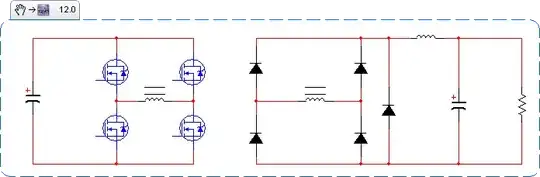
I'm in the process of building an 8kW isolated DC/DC converter, full-bridge topology. enter image description here

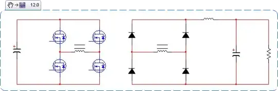
I'm seeing some interesting phenomena on the diodes. When each diode becomes reverse-biased, a voltage spike appears across the diode, before settling down to the expected DC bus voltage. These are 1800V fast diodes (320nS spec'd recovery time), and the spikes are hitting 1800V with only 350VDC on the secondary, well below my output voltage target. Increased deadtime doesn't help; the kick still appears when the diode is reverse-biased, and is just as large.

My suspicion is that the output choke is keeping the diodes forward biased during the dead time. Then when the transformer voltage starts to rise in the other half-cycle, the diode gets instantaneously reverse-biased long enough to appear as a short across the transformer winding. Then when the diode recovers, that current is cut off, causing the kick I'm seeing.

I've tried a few things. At one point, I added a flyback diode in parallel to my bridge. enter image description here I used the same fast-recovery diodes as are in my bridge. This had no apparent effect on the spikes. I then tried adding a .01 uF cap in parallel to my bridge. enter image description here

This reduced the spikes to a more manageable level, but the reflected impedance of that cap caused significant problems on the primary. My snubber caps have doubled in temperature!

A few possibilities present themselves:

1) I've diagnosed the problem incorrectly. I'm 95% sure I'm seeing what I think I'm seeing, but I've been wrong before.

2) Use a synchronous rectifier. I shouldn't have reverse recovery issues with that. Unfortunately, I'm not aware of any reverse-blocking JFETs in this power range, and there's no such thing as a reverse-blocking MOSFET. The only reverse-blocking IGBTs I can find in this power range have worse losses than the diodes.

EDIT: I've just realized I've been misunderstanding the nature of a synchronous rectifier. I don't need reverse-blocking FETs; the FETs will conduct drain-source.

3) Use zero-recovery diodes. Again, problems with losses and cost.

4) Snub the kicks. This looks like it would eat way too much power, on the order of 20% of my overall throughput.

5) Add saturable cores in line with the diodes. Two of the largest saturable cores I could find barely dented my kicks.

6) Use a zero-current-switching resonant topology. I have no experience in that area, but it sounds like if the current on the primary changes more smoothly, the voltage on the secondary should also change more smoothly, giving the diodes more time to recover.

Has anyone else dealt with a similar situation? If so, how did you solve it? Edit: primary-side FET datasheet here.

Stephen Collings
  • 17,373
  • 17
  • 92
  • 180
  • 1
    have you tried RC snubber and/or large ferrite beads which also have the effect of ~ ~100pF loading at same time as real impedance absoprtion of RF transients. – Tony Stewart EE75 Dec 21 '12 at 22:13
  • 1
    Do your primary MOSFETs have fast body diodes? Are you using a hard-switching topology, or one of the ZVS variants? – Adam Lawrence Dec 21 '12 at 22:45
  • Which diodes are you using? Could you link to a datasheet? –  Dec 21 '12 at 22:54
  • I've added FET and diode datasheets. Hard switching, no ZVS. I've tried a ferrite bead, which had no apparent effect. It was picked because it was at hand, not for its specs, so its possible it's just woefully undersized... nice to know the idea is reasonable... – Stephen Collings Dec 22 '12 at 04:13
  • Where would you suggest the RC snubber? – Stephen Collings Dec 22 '12 at 04:13
  • What would happen if you replaced each diode with a series diode+inductor combination? Perhaps start with 4 inductors, each one identical to the output filter inductor you already have? – davidcary Dec 22 '12 at 08:12
  • Can you show any decent coaxial RF measurements? or using Differential probes with short ground clips? You know if it is decent for crosstalk if when you prbe the ground signal or AC connect to neutral and probe you get a null signal with zero spikes. – Tony Stewart EE75 Dec 22 '12 at 11:21
  • Also pls specify transformer turns ratio and inductance at 1MHz on primary or give PN and same for all caps used (PN's) – Tony Stewart EE75 Dec 22 '12 at 11:32
  • What is your budget? I posted a workable snubber and inverters BOM cost target? – Tony Stewart EE75 Dec 22 '12 at 14:46
  • 1
    What is the non-spike worst case reverse voltage seen by the rectifiers? (The so-called plateau voltage). If your plateau is low enough, you could try and use 1.2kV SiC Schottky rectifiers, or if those aren't good, a lower voltage conventional rectifier with lower reverse recovery charge and a smaller RC snubber than your 1.8 kV solution requires. – Adam Lawrence Dec 22 '12 at 15:54
  • Plateau voltage is max 1250. I have 1700v SiC diodes on hand, but thermally they're borderline possible. Snubbing is probably preferred at this point. Budget is TBD. I'm building the prototype so we can decide if production is even feasible. – Stephen Collings Dec 22 '12 at 19:32
  • Back on site. I looked at the line of beads we typically use, http://www.toshiba-tmat.co.jp/eng/list/am_am.htm, AMOBEADS from Toshiba. I'm not 100% clear on my translation of the pseudo-English, but I think my idea of "woefully undersized" was right. 230 nS recovery x 1250V = 288 uW. The biggest one they make is under 10 uW. SO! Snubber. – Stephen Collings Dec 27 '12 at 14:17
  • Wow! No, you're right; 10-20% loss in the snubber is far too high! The snubber absorbs a constant amount of energy per event : more events per second = more power. I think the problem is that your switching frequency is high - throughout this discussion so far, nobody has asked how fast you are switching. So I'll ask ... what is your switching frequency? You may have to increase the R in your snubber; find some way to mitigate the reverse recovery charge (would series diodes help?) or tune the design for lower frequency. Or... –  Jan 11 '13 at 10:29
  • Or ... is there any way to dump those spikes into the appropriate output rail? –  Jan 11 '13 at 10:30
  • I'm switching at 20-40 kHz, depending on the day. I can drop as low as 12 kHz if I really have to, but I'd rather not. Dumping the spikes to the output rail is an interesting idea. I'd have to use zero-recovery diodes, for the speed, and then somehow have the slower ones take over for the majority of the output pulse. They may naturally share anyway, since the zero-recovery diodes have much higher forward biasing... that's worth a look. – Stephen Collings Jan 11 '13 at 14:29
  • 1
    Have you considered non dissipative snubbers..? –  Feb 25 '14 at 18:18

3 Answers3

17

Flogging the FREDs

Voltage fed converters with transformer isolation will exhibit ringing in the secondary. Ringing is caused by parasitic inductances and capacitances in the circuit, with the dominant elements will being the transformer leakage inductance (\$ L_ {\text {Lk}}\$) and junction capacitance ( \$ C_j\$)of the bridge diodes. The diode data sheet shows \$ C_j\$ of 32pF. I'm going to make a naive guess at \$ L_ {\text {Lk}}\$ of 500nH, but it will have to be measured to really know. So, an LC of 500nH and 32pF is what must be snubbed.

Spike amplitude without snubbing will be \$ 2 n V_ {\text {in}}\$, where \$ n \$ is transformer turns ratio and the factor of 2 is what you get for a high Q resonance.

There are different types of voltage snubbers; Clamping, Energy transfer resonant, and Dissipative. The clamping and resonant types require more parts and some involvement of active switches which I think make them impractical for this case. So, I am only going to cover dissipative snubbers because they are the most simple and work well with passive switches (like diodes or synchronous rectifiers).

The form of dissipative snubber that I will cover is a series RC placed in parallel with each bridge diode.

Some facts about RC dampening snubbers:

  • They are all about impedance matching. You don't get to choose the snubber resistor value \$ R_d\$. The parasitic LC determines that for you by characteristic impedance Zo.
  • You do get to choose the value of the snubber cap \$ C_d\$. That's important since the cap value sets the snubber loss (\$ P_ {\text {Rd}}\$)as \$ C_d F V^2\$ . Where V is the pedestal voltage and F is switching frequency. The snubber cap must provide a low impedance at the LC resonance of the parasitics, so it needs to be several times \$ C_j\$.

Some guidelines, and what to expect with RC dampening snubbers:

  • For \$ L_ {\text {Lk}}\$ of 500nH and \$ C_j\$ of 32pF, Zo will be 125Ohms. So, \$ R_d\$ would be 125 to match Zo. You may have to fine tune this a little since \$ C_j\$ is non-linear and falls off with reverse voltage.

  • Choosing the snubber cap \$ C_d\$ : Choose \$ 3 C_j\leq C_d\leq 10 C_j \$ . Higher values in the range do provide better dampening. For example, \$ C_d\$ of \$ 3 C_j\$ will result in a peak diode voltage of \$ 1.5 n V_ {\text {in}}\$, while \$ C_d\$ of \$ 10 C_j\$ will result in a peak diode voltage of \$ 1.2 n V_ {\text {in}}\$.

  • Dissipative snubber performance will not improve for \$ C_d\$ values greater than \$ 10 C_j\$.

Power loss \$ P_ {\text {Rd}}\$, with a pedestal voltage of 1250V and F of 50KHz.

  • If \$ C_d\$ is \$ 3 C_j\$ or 100pF, \$ P_ {\text {Rd}}\$ = \$ C_d F V^2\$ or 7.8W.
  • If \$ C_d\$ is \$ 10 C_j\$ or 330pF, \$ P_ {\text {Rd}}\$ = \$ C_d F V^2\$ or 25.8W.

\$ C_d\$ of \$ 10 C_j\$ gives the best dampening with peak voltage of 1.2 time the pedestal voltage, but you can save some power with smaller snubbing caps if you can stand the higher peak voltage.

gsills
  • 7,133
  • 16
  • 22
10

This is a classic snubbering problem. A diode can't instantaneously go from conduction to blocking; the charge in the PN junction needs to get swept out, and an RC snubber across each diode should help this.

I used to design industrial soft starters and on the medium-voltage units we had a lot of design work around this particular aspect. It's been a long time since I've worked in this particular industry so I don't recall the snubber values, but I would probably start with 0.1uF and maybe 49 ohms and see where things start shaking out from there.

akohlsmith
  • 11,162
  • 1
  • 35
  • 62
  • 1
    +1. Yes, this sounds like a "high frequency ringing at diode turn-off" problem, and a snubber is a good fix. [a](http://eclipsedt.com/2011/02/multiphase-48-volt-conversion-for-low-noise-applications-in-an-instrument-grade-power-supply/) [b](http://www.hagtech.com/pdf/snubber.pdf). – davidcary Dec 22 '12 at 08:36
  • yes but what kind of snubber – Tony Stewart EE75 Dec 22 '12 at 14:46
  • @Richman I would start with a 0.1uF capacitor and a 3.9 ohm, 2-5W resistor in series with the cap across each diode. The power rating is just a guess, you would have a better idea than me. (edit to use Brian Drummond's calculated value) – akohlsmith Dec 22 '12 at 17:21
  • I'll try this when I'm back in the lab Thursday. – Stephen Collings Dec 22 '12 at 19:33
  • 2
    .1 uF + 2 ohms knocked down my kicks nicely. However, my snubber resistors are taking a beating. 100W resistors are reaching temp limit very quickly, and even two in series (4 ohms 200W total) still overheated. It seems a little ridiculous to be spending 10% of my power budget just on snubbing the diodes. Snubber design not being something I've spent much time on, I'm not sure if there's an obvious path forward, or if this is just the cost of doing business. Does anyone have other suggestions? – Stephen Collings Dec 27 '12 at 18:55
  • 1
    I just went back over some of my old notes. We used .47uF and between 25 and 75 ohms, depending on the specific SCR. The snubbers were big because of the power requirements, but we had the advantage that we were typically only in-circuit for 60s or less (soft starting). – akohlsmith Dec 31 '12 at 13:49
  • Yeah, that helps. We're looking at running 8 kW continuous, though, so having snubber losses >1kW really isn't going to work! I'm presently exploring making a ZCS resonant converter, which I think will eliminate my voltage kicks. Any thoughts on that? – Stephen Collings Jan 01 '13 at 15:05
  • I've unfortunately never worked on ZCS converters so I don't have any resources or experience to draw on. I'm familiar with the basic concept, but can't really offer much in the way of recommendations or suggestions. – akohlsmith Jan 01 '13 at 17:22
5

60A reverse recovery current! (from the datasheet) That has to go somewhere...

Like Andrew Kohlsmith, my first thought would be an R-C snubber across EACH diode, but I'm reluctant to make that an answer unless you can find precedents at similar power. Andrew seems to have the experience to make that judgment; not having worked on industrial power, I do not!

But let's run some numbers : as your forward current will average something like 25A (8kw,350V) let's use the same value for Irm - 25A * Trr=230ns gives a ballpark stored charge of 5.75 uC, which would charge up an 0.1uf capacitor to a more manageable 57V. But 25A * 49R is a bit high (!) - this crude calculation would suggest 4 ohms (or even 2) rather than 49 as a starting point for the snubber resistor.

I repeat : I have not worked on industrial power, so that's just what the numbers say to me. I would appreciate Andrew's commentary given these numbers.