1

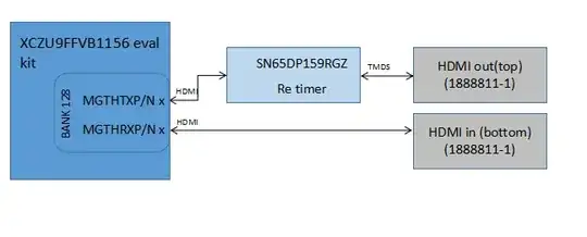
I am exploring a Zynq ultrascale+MPSoC design. While looking at the reference design of XCZU9FFVB1156 SOC evaluation board, in the HDMI interface there is a retimer IC in the transmitter side of Bank 128, which converts the HDMI signal to TMDS along and routed to HDMI output port. But in the receiver side, no such signal enhancing or TMDS to HDMI circuit is used.

I have attached the snapshot of my observation from the evaluation board design for reference.

Why is there no retimer or similar circuit in the HDMI input port? Please can you clarify the concept.
block diagram

SamGibson
  • 17,231
  • 5
  • 37
  • 58
BalkisMM
  • 47
  • 2

2 Answers2

1

The Xilinx HDMI PHY TX implementation probably can’t meet the timing spec for higher resolution modes (e.g., 4Kp60) so it needs to be re-timed. The re-timer also does TX pre-emphasis to improve signal integrity at the receiver side.

The receive side has no such issues since the obligation to meet timing and SI is on the TX and connection cabling. As long as the RX thresholds and margins are met it will work. Internally the deserializer does its own kind of retiming.

hacktastical
  • 49,832
  • 2
  • 47
  • 138
0

A retimer is usually used for many reasons.

Usually the reason is that the direct high speed interface pins on some device has incompatible voltage levels or need AC coupling to the next device, so it must be received and retransmitted with voltage levels and DC coupling which HDMI requires to work. The retimer output can also have a stronger drive strength to be able to drive longer cables, and the retiming function can clean any jitter on the input, so the signal quality is higher and it can be better received over longer cables due to that reason too.

Justme
  • 127,425
  • 3
  • 97
  • 261