0

Continuing with my edge triggered ramp generator and its simulation, thanks to all your help I have the LTspice simulation set up that I can see a theoretical circuit work that uses the rising edge of the inverted ripple-carry output (RCO) at the end of a counter to trigger the ramp generator.

enter image description here

This is all jolly nice, but of course the currents of over 2A involved here are completely nuts. So, I put in what I computed the right values for Rhigh and Rlow of that 74LS04 TTL inverter that I'm using:

enter image description here

  • Rhigh = 5V / 0.4mA = 12.5kΩ
  • Rlow = 5V / 16mA = 312.5Ω

and when I use these values, of course I can not ever properly discharge that capacitor C1.

enter image description here

So, I need some other trick to rip the current valves wide open based on a little triggering butterfly flapping its wings. I think I know what I will try. That's this feed-back coupled NPN-PNP pair instead of my simple NPN:

enter image description here

I know it's ridiculous, a screen shot from a video, of a guy filming an old book. But hey, this seems like the most applicable solution for me and I take'em where I find'em.

my annotation arrows are my own guessing. In fact I don't understand how that "end of period reset" transistor pair would work. since it seems like the entire discharge current of the (selectable) capacitor needs to flow through the base of the NPN transistor.

So I focus on the triggering side there. But there it's the same thing, in the end the current needs to be queezed from the collector of the PNP through the base of the NPN in order to go to ground. But at least here the base current of the PNP takes the collector-emitter path of the NPN and helps out.

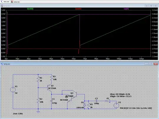
I'm probably still not quite clear about all of this. So I took another video where it's simpler and the guy explains it better. So I came up with this here:

enter image description here

and as you can see, I tweaked the TTL inverter parameters again because I have positive proof that the edge detection circuit works from my earlier exercise, and the proof is in the scope pictures here: How do I make a 74LS170 or 74LS670 register file reliably clock in data on the rising edge?. So, TTL signal edge detected, I can only get this over the TTL threashold if I reduce the Rhigh value from 12.5kΩ to 0.5kΩ.

I am incredulous about this, as it again shows high current peaks through C2, but in practice I showed it works. And so I take that same 0.5kΩ for the positive edge detection to be inverted again, so that the down-spike should now open the Q2-Q3 pair to drain C1 quickly.

But I am still confused now how I should correctly estimate the TTL impedances to high and low, because I am doubting that I can sink enough current during low on A2 to open that Q2-Q3 pair.

What say you?

PS: I will now simplify my positive edge detection RC to a negative edge detection RC, which I have built for an EEPROM programmer. Perhaps I don't need these TTL gates after all...

PS: here is my ramp.asc if anyone wants to play with the same:

Version 4
SHEET 1 1420 680
WIRE -64 -144 -240 -144
WIRE 96 -144 -64 -144
WIRE 96 -32 96 -64
WIRE -240 0 -240 -144
WIRE -64 16 -64 -64
WIRE 32 16 -64 16
WIRE 96 96 96 64
WIRE 208 96 96 96
WIRE -64 128 -64 16
WIRE 96 144 96 96
WIRE 352 144 272 144
WIRE 448 144 352 144
WIRE 640 144 512 144
WIRE 688 144 640 144
WIRE 752 144 688 144
WIRE 880 144 816 144
WIRE 1008 144 944 144
WIRE 288 192 208 192
WIRE 640 192 640 144
WIRE 688 192 688 144
WIRE 1008 192 1008 144
WIRE -240 272 -240 80
WIRE -64 272 -64 208
WIRE -64 272 -240 272
WIRE 96 272 96 208
WIRE 96 272 -64 272
WIRE 352 272 352 240
WIRE 352 272 96 272
WIRE 640 272 640 256
WIRE 640 272 352 272
WIRE 688 272 640 272
WIRE 1008 272 688 272
WIRE -64 304 -64 272
WIRE 800 464 768 464
FLAG -64 304 0
SYMBOL res -80 -160 R0
SYMATTR InstName R1
SYMATTR Value 2.2k
SYMBOL res -80 112 R0
SYMATTR InstName R2
SYMATTR Value 10k
SYMBOL res 80 -160 R0
SYMATTR InstName R3
SYMATTR Value 12k
SYMBOL cap 80 144 R0
SYMATTR InstName C1
SYMATTR Value 470p
SYMBOL pnp 32 64 M180
WINDOW 0 60 74 Left 2
WINDOW 3 28 42 Left 2
SYMATTR InstName Q1
SYMATTR Value BC556B
SYMBOL npn 288 144 R0
WINDOW 0 52 21 Left 2
WINDOW 3 31 53 Left 2
SYMATTR InstName Q2
SYMATTR Value BC546B
SYMBOL voltage -240 -16 R0
WINDOW 123 0 0 Left 0
WINDOW 39 24 124 Left 2
SYMATTR InstName V1
SYMATTR Value 5
SYMBOL voltage 1008 176 R0
WINDOW 3 44 86 Left 2
WINDOW 123 0 0 Left 0
WINDOW 39 0 0 Left 0
SYMATTR InstName V2
SYMATTR Value PULSE(0 5 0 0 0 500n 64u 100)
SYMBOL Digital\\inv 944 80 M0
WINDOW 3 -261 7 Left 2
WINDOW 123 -245 -19 Left 2
SYMATTR InstName A1
SYMATTR Value Vhigh=5V Rhigh=312.5
SYMATTR Value2 Vlow=0V Rhigh=0.5k
SYMBOL cap 816 128 R90
WINDOW 0 0 32 VBottom 2
WINDOW 3 32 32 VTop 2
SYMATTR InstName C2
SYMATTR Value 22p
SYMBOL res 672 176 R0
SYMATTR InstName R5
SYMATTR Value 1k
SYMBOL diode 656 256 R180
WINDOW 0 24 64 Left 2
WINDOW 3 24 0 Left 2
SYMATTR InstName D1
SYMBOL pnp 272 192 R180
WINDOW 0 55 77 Left 2
WINDOW 3 24 44 Left 2
SYMATTR InstName Q3
SYMATTR Value BC556B
SYMBOL Digital\\inv 512 80 M0
WINDOW 3 -261 7 Left 2
WINDOW 123 -245 -19 Left 2
SYMATTR InstName A2
SYMATTR Value Vhigh=5V Rhigh=312.5
SYMATTR Value2 Vlow=0V Rhigh=0.5k
TEXT -274 328 Left 2 !.tran 96u

UPDATE: well, I just built one with a N-MOSFET

enter image description here

the trick here is the MOSFET with very low threshold required and pretty low resistance. But it is built from a real part that I might get.

UPDATE: or I stay at home and use what I have, just do the good old Darlington pair. Thanks to my explorations in power amplification.

enter image description here

Gunther Schadow
  • 1,441
  • 7
  • 22
  • 2
    You know? I'm starting to want to go back to ground zero and just ask you again to write out what you are trying to achieve, end to end. (Not stuff in the middle.) What are you doing, actually? Forget the circuit stuff. Are you generating composite? NTSC? PAL? VGA? ... Why? From what, exactly, to what exactly? Do you need to support multiple video output formats? Or just one? What's generating the frames that you want to display? I mean, really get back to zero. – jonk Aug 24 '20 at 21:58
  • 2
    I feel like I'm being asked to help "hack" around until some random combination of ideas manages to in some Rube-Goldberg way finally work, kind of. When instead one should be forced to just sit down and work out an honestly thoughtful approach, run it by others to make sure it's a good one for solving the problem, and all this ***before*** starting to put any hands onto parts in order to test and make things. – jonk Aug 24 '20 at 21:59
  • @jonk, I am learning. a self-student of electronics. I want to know how stuff works. I want to reproduce basic methods. If you have followed all my questions around (which appears you did) you will see I have dabbled in audio amplifiers and in digital, building a CPU, building an oscilloscope screen output, you see how I did that with a DAC and now I want to do it with analog ramps. Someone told me on my question about the DACs that I couldn't do a raster screen that way -- well, I could! But I still want to try the ramps. I made Conway's Game of Life on the o'scope. I'm learning by doing. – Gunther Schadow Aug 24 '20 at 22:34
  • I don't mind learning and self-education. (I'm all about that, in fact.) But I think it's just difficult (at least, it is for me) to figure out where best to offer suggestions. I don't know what to suggest for this circuit you are looking at. I could write stuff about it, but I wouldn't know why I was or what I could say that might help. I perceive you think things about it that are wrong. So just writing without dealing with those, seems wasted. Yet telling you to do something else also seems wasted, because this is what you want right now. So I guess I'm stuck waiting for you to move on. – jonk Aug 24 '20 at 22:43
  • @jonk, haha, well, I guess my questions are too long winded then. The summary is (a) how to set up CORRECT parameters for TTL chips in the simulator, so I capture their real current properties correctly? (b) my original question about the ramps was and still is: how can I reset the ramps at the end of a counter? You could say: why do you even bother with the RCO, you could just detect the falling edge of the MSB! And you'd be right. But I still need to drain that capacitor based on the falling edge of a TTL line. – Gunther Schadow Aug 24 '20 at 23:43
  • (a) You could create the standard output using actual BJT parts and resistor values. The schematic is well-documented and I've detailed how it works, here, as well. Or you could write only a behavioral model using generalized Spice tools to create a more idealized version. Either way, you could package that up into a .SUBCKT and just stamp them out when needed. (b) You could also detect when the ramp reaches a voltage, using a self-triggering SCR schematic and do it that way, as well as other ways. Which of course gets back to knowing why you want something, and for what, etc. – jonk Aug 25 '20 at 00:44
  • @jonk I want the ramp(s) to drive my o'scope's X and Y. Hence ~15 kHz (64 μs) for one ramp, and 60 Hz for the other. The 60 Hz is simple. I am going to split out two more questions, hoping tat simpler questions might help simpler answers without too much worrying about the ultimate goals. – Gunther Schadow Aug 25 '20 at 00:50
  • If you just want a simple 15 kHz ramp, and it doesn't have to be precisely 15 kHz (you don't need a counter for that), then there's lots of really simple ways to go. Just set up a 555 timer to set up 15 kHz, feed that to a FF with Q and /Q to get 7.5 kHz, use that as shown in my schematic, and be done with it. If you want the ramp only 50% of the time, eliminate a diode and a resistor and a capacitor. And that's more complex than it needs to be, I guess. You could just directly use the 555 with whatever duty cycle seems appropriate, set up a current source, and you are done. – jonk Aug 25 '20 at 01:15
  • I am just looking again at your circuit here: https://i.stack.imgur.com/6ngrz.png and what I am most curious about is how you replaced R1 with a normal diode and a zener. So this R1 is really a very finicky thing apparently. The guy showing his old book in the video also has a couple of diodes in that place of my R1. – Gunther Schadow Aug 25 '20 at 01:40
  • That's a 6.8 V zener. That voltage, in particular, has some special attributes with respect to temperature and how it combines with the rest (BJT and other diode) for some semblance of temperature stability. You can use a resistor, if you want. It's just not so good if you apply a heat gun to the thing. – jonk Aug 25 '20 at 01:46
  • @GuntherSchadow That's a [Zener current source](https://en.wikipedia.org/wiki/Current_source#Zener_diode_current_source), the only difference being they used NPN instead of PNP. The more stable the current, the better linearity of the ramp. – a concerned citizen Aug 25 '20 at 07:30

0 Answers0