0

PWM Attiny45 Motor Controller

I made a PWM Motor Controller with a Attiny45. I have a few questions regarding each section of my schematic. This design is for 40A/18V, so 720W. I know this is beyond my current skill and I take full responsibility for burning things, I try to be careful.

1. VCC / DC-DC Converter

I just took the recommended design and I hope everything is okay. If someone finds a error, let me know.

2. Battery Control

This is optional, ignore please.

3. Attiny IC

This also seems pretty straight forward, I hope I did not make any mistake.

4. Motor Control

Can I use the MCP1416T-E/OT with 5V PWM IN and 14-18V VCC together with two parallel NCE2030K MOSFETs? Is it even possible to use two MOSFETs parallel? I often see designs where there is a 100k resistor from gate to source. Is that necessary here?

Thank you for your help, I tried to keep the design simple.

Voltage Spike
  • 75,799
  • 36
  • 80
  • 208

2 Answers2

3

The MOSFETs used for controlling the motor are rated at 20 volts maximum voltage and this, in my opinion is too close to the nominal 18 volts supplied from your 18 volt battery. I would make the MOSFET maximum voltage more like 30 volts.

If the 40 amp current perfectly shared for each MOSFET then that would be 20 amps per device. However, the MOSFETs will get warm and this will raise their temperature and raise the on-resistance possibly to around 30 mΩ at a junction temperature of above 100 °C. This will dissipate (in each MOSFET) a power of 20² x 0.03 watts = 12 watts and I don't see anything about the copper-area heatsinking you might have formed on your circuit board.

I am also concerned that the data sheet isn't clear about the safe operating area especially at longer on-periods other than 1 ms: -

enter image description here

The 32 amps and 1 volt lines indicate an on-resistance of about 30 mΩ.

I would strongly urge you to look at data sheets from other (more recognized) suppliers to see how the safe operating area curve might be applied for longer on-duration periods.

You need to work on this if you haven't considered it. You also need to reckon that the MOSFETs won't equally share current so I would use a 2:1 factor for this and this suggests to me that the maximum continuous current rating of 30 amps (per MOSFET) is inadequate.

The back-emf protection (D3) isn't clear in your schematic. This also needs to be rated for well-over a peak current of 60 amps in my opinion.

Andy aka
  • 434,556
  • 28
  • 351
  • 777
1

Here are some points that I remarked on your schematic

What is the minimal set of parts for a circut with this AVR microcontroller?

Atttiny and Atmega are from same family and I would recommend using pull-up on your reset pin. You are driving motor, then unwanted EM inteference is abound and your controller will most likely trip a reset bar. It wont be constantly held up by your programmer (I hope)...

Battery control section ignored as requested.

DC/DC Converter LM2596 is prone to oscillation in some cases, according to book Switching Power Supplies A-Z by Maniktala (easy to find book, but information buried in it somewhere). Keep an eye on this bugger if possible.

100k Resistor is there to provide current charging to Miller Capacitor that is present in MOSFET (inherent in construction of MOSFET). Some use it, some don´t depending on case. WIth Gate driver, I would give a small resistor 100R or similar, just to limit current flowing into MOSFET. Optimisation is desired after working prototype (check resistor thermal rating).

I haven´t done calculation on MOSFET disssipation, but answer from Andy aka "seems leg´t" so take care on thermal side here (heatsinks, heatsinks, heatsinks). If you want to avoid this you can just stack mosfets (as you did) to get sufficient power divider to lower dissipation on each. This is not elegant solution, but sometimes brute force is fun and good for learning.

I would put a pull down resistor on gate pins, to prevent any accidental "switch on"s during power up phase. I recommend 47k to 10k. No preference on any of those, just sufficient pull down to ground. 100k is not recommended as they can be considered "too weak pull down".

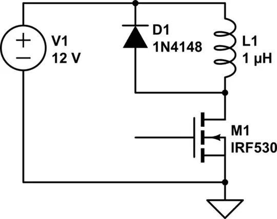
You need to have inductive kick-back diode present as well. Sure this was mandatory for BJT and you can get away without putting one on MOSFET because of "built-in" MOSFET body diode, but I always prefer to have my own components instead of hoping for built in failsafes.

Here is link to this discussion.

Where should I put the kickback diode in a transistor switch?

This was "back of envelope calculation and design" so let know if you need any additional information

Happy hunting and remember - safety first