Take Two: update
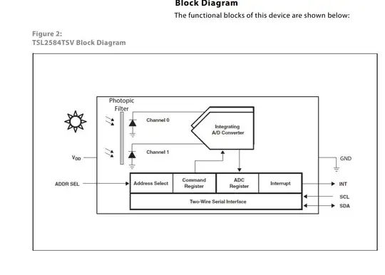
Since these Photo diodes act as current sources, only single integration is needed, so they are done in parallel.
- unlike a traditional multi-channel DMM* with dual slope = fixed time integration up then voltage dependant Time measuring integration down for best noise immunity of a noisy voltage.
The integration time is programmable in the counter registers. The result is an 8bit result with optional gain control. Except the highest gain is weird. Instead of putting the decoupling cap close to the chip, they want you to put it farther away as the trace inductance 0.5 to 1 nH/mm affects the gain error. To get so called gain=111x that is actually the farthest distance in the graph of L vs Distance to decoupling cap. They average the gain of both channels VIS + IR or Ch 0&1
(116 + 106.5)/2= 111x gain
This could be related to resonance in the IDC cap dump voltage error interacting with decoupling cap and low Ron low L series resonance on using Vdd for VRef for ADC conversion.
Although it’s possible they are doing something fancier and counting pico coulombs and dumping for each count while integration up to =≈2/3 second so single stage IDC converters x2ch
So it is a dual ADC design but anyway they don’t really want to tell you how they do it.
===============.
Initial guess
Consider it as two parallel integration 8 bit counters that interpret this as a Dual Slope Integration ADC with a 2 port input analog MUX.
This could be a very useful E/W azimuth detector for a PV servo. But upon reading the specs, I see it is an CIE eye corrected filtered PD on 1 ch. and an IR filtered PD [photo diode] on the other.
The first block is a many channel MUX to ADC.

