16

I am finishing a PCB and I wanted to add some kind of artwork in my PCB, but not just import an image, I was thinking about placing some lines in the silkscreen, but I didnt wanted it to cover the other things in the silkscreen plane. I wanted it to behave like the Polyogn Pour, or even better, like the inverted, were the lines (or a fill) were on top of some text, the text wil invert the colors. Is this even possible? Tips about cool artwork things to do in Altium are welcomed as well.

EDIT:

Example of what I am aiming for, the white stripe is a random image and as it touches the components names, they will still be readable, since their color will automatically change, i.e. the software will remove the silkscreen overlay from the intercepting parts (or maybe make a full rectangle around the names to protect them, which I didnt present in this example but I think its easy to imagine).

enter image description here

mFeinstein
  • 4,293
  • 11
  • 45
  • 84
  • I tried something similar in Target3001! and the result I got by exporting DXF file of silkscreen and then edit it and merge with artwork. Later import DXF with silk + artwork and place it on silkscreen layer. – Malic Nov 30 '16 at 15:46

3 Answers3

37

The kind of exclusionary silkscreen pour you're asking for in the question is a cool idea, but as far as I know Altium doesn't have the facilities for doing that.

Anyways, the Altium documentation has a pretty good workup on how to add images to various layers.

Also, it's supposedly possible to paste various types of content (images, MS Word charts, etc...) directly into a PCB, but I was not able to get that functionality to work for me. I suspect it requires you have MS Office installed, and I use LibreOffice instead.

Anyways:
enter image description here
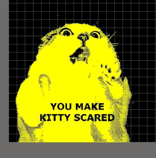
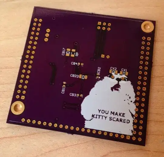
It's worth noting that the above picture made my processor absolutely crap it's pants (And I'm using a fast Core i7, so it's not a lack of available CPU.). The original artwork was only 440*400 pixels, so it seems smaller images are a very good idea.

Later note: I tried to get the above image into a actual PCB, and had no luck. Trying to do anything (even simply dragging) to the image primitive basically caused Altium to lock up and become unresponsive, and after a few minutes, I killed the process. I wound up having to reduce the image to black & white, and ~150*100 pixels to make it manageable.


Edit:

I think that, theoretically, it should be possible to define a polygon using a 2D DXF or DWG file. If you do that, it may be possible to get the behaviour you want (pull-back from existing art). However, you would need to convert whatever art you want to insert onto the PCB into a vector format, and then to a DXF/DWG file. I don't have the software to try that on my computer. Sorry.

Further edit:
Found it - "Define Polygon Shape from Selected Objects"

You can create company logos or polygons easily from external sources (i.e., DXF or AutoCAD ® ) using Define a polygon from selected objects in the PCB Editor.


Ok, this is totally happening:

enter image description here
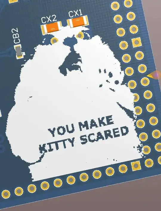
Yes, the positioning of the crystal pins in the eyes is deliberate.

As an amusing aside, silkscreen art like this appears to be an excellent way to break various DFM tools. So far it's managed to break the OSHpark.com upload tool. We'll see how it works with the Advanced Circuits FreeDFM tool.


SO IT'S A THING NOW:

enter image description here

Connor Wolf
  • 31,938
  • 6
  • 77
  • 137
  • I thought about that, but that means I would be spending too much time going back and forth for just one simple component replacement operation... – mFeinstein Dec 13 '12 at 14:43
  • 2
    +1 for awesome kitty. I need to add that to my boards – Gustavo Litovsky Dec 13 '12 at 17:19
  • 8
    Vias for eyes were a nice touch – bhillam May 29 '13 at 04:29
  • @Connor Wolf I just saw the edits now haha the PCB looks great! But unfortunatly thats not what I was aiming for, I placed a better example in the original post. – mFeinstein Nov 13 '13 at 05:37
  • @mFeinstein - I kind gathered what I posted wasn't precisely what you were asking for. I don't know if there is any way to do what you're asking, unfortunately. – Connor Wolf Nov 13 '13 at 06:57
  • -1 for kinda not answering the question and getting carried away. +2 for kinda not answering the question and getting carried away - in an awesome way. – RedGrittyBrick Nov 13 '13 at 10:13
  • 1
    @RedGrittyBrick - In my defense, the original idea happened before the OP had clarified, and I couldn't exactly *not* post the rest at that point, could I? – Connor Wolf Nov 13 '13 at 10:47
  • Looks more like a badger in monochrome :) –  Nov 30 '16 at 15:53
8

I used manual rotoscopping for these things (cad in transparent mode with picture beneath). Don't have the board pic right now, but that's how it looked in cad (colors differs from real board a bit, so it looks kinda strange).

bassist

hitomi2500
  • 81
  • 1
  • 1
6

Well for all those who wanted to know weather this is possible look at this:

enter image description here

frigging amazing

Nick Alexeev
  • 37,739
  • 17
  • 97
  • 230
anon5656565
  • 61
  • 1
  • 1
  • 2
    Welcome to Electrical Engineering StackExchange. Your answer isn't very helpful unless you can discuss the details of this example and how it was done. Please provide more instructive information in the answer. – Joe Hass Dec 03 '13 at 02:08
  • The PCB is from [this project](http://casperelectronics.com/finished-pieces/nova-drone/). No information on how the artwork was done though. – Matt B Dec 03 '13 at 04:22
  • This PCB has what I was looking for, image and preserved labels, which ECAD did the designer use? I really wanted it in Altium... – mFeinstein Dec 04 '13 at 12:51
  • The schematic on the linked page was drawn in Eagle. Not sure how the silk effects were done. – Connor Wolf Oct 02 '14 at 15:47