0

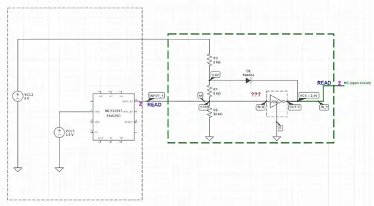
I'm studying the a circuit that is using a driver ULN2803 datashet. The driver is needed for external loads as LEDs when a pin is writing. The situation that I would like to talk about is when the pin is reading. As the GPIO interface is MCP23s17 datasheet, when pin is an input, pin gets Z state.

To explain the enterely application could be a mess, I will try focusing the description on the doubt about ULN2803 behavior within the circuit.

I'm new using it. I have used it for inductive loads, as relays, application once before. I thought I understood the most of this device. But after working with this circuit I realize that I miss some important things.

enter image description here

schematic

simulate this circuit – Schematic created using CircuitLab

I think the most important involved circuit is inside the green box.

Maybe the circuit is not functional for what I need. But I was analyizing it over the paper and set on my breadboard and I don't get it of all. So I took some values. I'm studying the value at M node when the output driver pin 'OUT_C' (OUT_C = IN_1) is not connected, so Z.

The following values can be seen:

  1. V at (driver output) OutC = VCE = IN_1 = 2.4V
  2. V at M node = 1.5V (driver input)
  3. V at Diode IN4004 Anode = 2.9V

What I did not understand was how 1.4~1.5V were there (driver input). I actually need input driver to be having about 3V. I'm sure the device is working correctly and who was wrong it's me. The resistor values were firstly calculated in order to have V = 3.3V at M node if driver was OFF. I thought that if driver was OFF, no current drive, so it could be 3.3V at M node. Obviously I don't see that. But I need to understand these questions:

  • I guess the driver is ON but if it was, Vin(ON) = 2.4V. Maybe it is not.
  • How can M node achieve 1.5V. I don't see it. I even take into account internal driver resistors but I don't get 1.5V.
  • I don't see why Vdiode = 2.9V
  • I guess VCE = Vdiode - Vd = 2.9 - 0.6 = 2.3V

Feel free for answering where the mistakes are and tell me what is wrong.
Suvi_Eu
  • 777
  • 6
  • 19

2 Answers2

1

It looks as if it's behaving to specification.

A ULN2803 is not a three-state logic buffer as you've drawn it. It's a linear darlington transistor with an open collector. That means it needs about 1.4 V on the base to start turning it on.

Your 5 V VCC2 supply goes through a voltage divider string R1 R2 R3, that without D2 would turn the 2803 on. Its Thevnin equivalent at the input to the 2803 is about 3.3 V from 6.7k.

The 2803 will now turn on, pulling the R3 R1 junction down through D2. Obviously this will decrease the drive to the 2803, and it will start to turn off. It will reach equilibrium when its input is just turning it on enough for the current through D2 to provide enough input voltage to turn it on just enough. Those voltage values look plausible for exactly that.

Neil_UK
  • 158,152
  • 3
  • 173
  • 387
  • Lot of thanks. I draw the triangle symbol for expressing amplification. Sorry about the confussion. I have no doubt that drivers works correctly and I'm who has lost myself by the way. I've learned that we would just need a buffer in order to disconnect the driver when reading '1'. We would need it because driver turns ON with more than 1.4V, and M node must be > 2.8V. But also a minimal current is needed. I thought I could make decrease it with D2 and Koms resistors. One of my missings was to assume Vin(ON) = 2.4V as the minimal required for turning it ON, instead of a maximum value. – Suvi_Eu Jun 18 '20 at 06:54
  • So, @Neil_UK, there is something at your explanation that I need to clarify whether I understood it well or not. According your last paragraph: do you mean that 1.4V is due to the driver being ON or OFF? is it due it is not in equilibrium? If it could keep almost 3V at its input, it will be fine for the proposal. Maybe with other resistors values could the input voltage being 3.3V instead of 1.4V? – Suvi_Eu Jun 18 '20 at 07:37
  • @EugeniaSuarez The 1.4 V is due to the driver being in the linear region between fully on (when input is > 1.5 V) and fully off (when input voltage < 1.2 V). That's why I'm stressing it's not a logic buffer, it's a linear amplifier, and you're running it in the linear region. It's only because of the existence of this linear region that it can get into equilibrium. – Neil_UK Jun 18 '20 at 10:11
1

More important than the 12.9 K of resistance in a 2803 input are the two base-emitter junctions. See section 8.2 of your datasheet. They appear as two diodes in series, acting as a 1.2 V zener diode. This makes the network appearing across R2 to GND in your schematic a bit messy to calculate, but I think you'll see that it explains the node voltage.

AnalogKid
  • 16,865
  • 1
  • 13
  • 25