5

On MOSFETs with multiple source pins, is the so-called "Kelvin-connected source pin" connected any different internally? Or is it just like every other source pin?

enter image description here enter image description here

EDIT: Just to be clear, I am not asking what the Kelvin connection is for. I'm asking whether it is physically implemented any differently than the other source pins or whether it is just an extra regular, old source pin.

DKNguyen
  • 54,733
  • 4
  • 67
  • 153

5 Answers5

7

The Kelvin connection is basically a dedicated small signal connection straight from the SOURCE/EMITTER of the die, dedicated for control. The reason this is done as oppose to using the SOURCE/EMITTER which carries the main current is to mitigate inductive voltage changes on the gate-source/emitter when switching current.

As devices switch faster this inductive drop can be enough to turn the device in/off.

It can be compared to the Kelvin connections on sensing components (sense resistors, NTC/PTC) where their primary concern is to minimise measurement error due to additional voltage due to harnessing and associated current.

Consider the image below. A MOSFET and a gate drive as part of a H-Bridge. Essentially this is how you would capture the circuit, but this is not the complete picture:

enter image description here

The package will have stray inductance and equally a classic 3-pin FET/IGBT will have lead inductance, and poor layout can result in poor control.

enter image description here

With higher current or higher switching speed, the voltage developed across the stray source inductance will increase. A TO-247 will typically have around 20nH of D-S inductance, roughly speaking split in half per pin. With current of 100A switching in 200ns, the resultant voltage developed across this pin, \$V = L \frac{dI}{dt}\$ or 5V, while the gate is being charged or discharged, effectively reduces the voltage from the driver, reducing or limiting switching speed.

To mitigate this, manufacturers of devices for power applications provide an auxiliary Source/Emitter connection to permit gate voltage control without transient behaviour due to the main current carrying connection:

enter image description here

Typically this is done via an additional bondwire (thinner gauge as it does not need to carry current) onto the Source/Emitter pad of the die, routed to the auxiliary Source/Emitter pin.

enter image description here

From: CREE 1200V SiC Module teardown reverse costing report published by Yole Developpement - slideshare.net

Another example of the kelvin source connection:

enter image description here

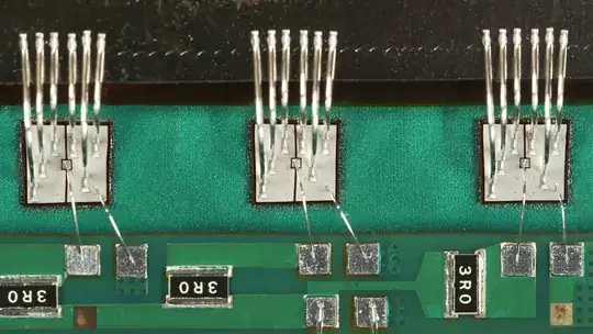
From: The Odd Couple: Silicon and Carbon Don’t Love Each Other. But When They Iron Out Differences, Their Marriage Can Be Revolutionary - GE

Tim Williams
  • 22,874
  • 1
  • 20
  • 71
2

You could search for "Kelvin source pin" on the manufacturer's web site.

Basically it's a Kelvin connection to the source itself, that bypasses any package parasitics that would screw up your control circuitry's measurement of the source voltage.

Google "Kelvin connection", and maybe "four wire resistance measurement".

TimWescott
  • 44,867
  • 1
  • 41
  • 104
  • I know what it's for. I'm wondering if it's wiring is differently internally from the other source pins. – DKNguyen Jun 11 '20 at 20:59
  • The app note that I linked to certainly implies that it is. – TimWescott Jun 11 '20 at 21:04
  • Hmmm. Where are you seeing that it is implied? The closest I see to that is Figure 1 where the Kelvin terminal bypasses the inductance LS2 and where it mentions that "large common source inductance...die to source wirebonds". However, none of those rule out that perhaps Kelvin connection's source inductance is actually identical to the other source pins and its inductance is just neglected because the di/dT it experiences is lower when wired as intended. – DKNguyen Jun 11 '20 at 21:16
  • 1
    That's what I was talking about. And yes, it could just be a bunch of identical pins. "Correct" (in my mind) would be an entirely separate bonding wire from the source, or a leadframe that's as solid as possible to the "main" source pins and slotted to the "Kelvin" pin. I wonder if you could just ohm it out? – TimWescott Jun 12 '20 at 04:39
  • I have the C3M on hand top one so I could try and Ohm it out tommorrow. – DKNguyen Jun 12 '20 at 04:42
1

Not an entire answer to my question, but I did find this which does indicate they are physically different, though it does not say why. enter image description here

DKNguyen
  • 54,733
  • 4
  • 67
  • 153
1

Take a look at the pictures in the previous posts showing bare dies with bondwires. The Kelvin Source terminal might be bonded with a smaller diameter bondwire. If this is used for the main current, it may fail.

Uwe Jansen
  • 11
  • 1
0

This is speculation, I've never heard of such a connection. My best guess is that it's like half a typical kelvin resistor connection. Aka the source pin (2) has high current carrying capabilities, while kelvin source (3) is same node but isn't designed to source significant current (only for voltage measurement purposes).

enter image description here

image source: https://en.wikipedia.org/wiki/Four-terminal_sensing#/media/File:Kelvin_connection_layout.png

Yet Another Michael
  • 2,052
  • 1
  • 10
  • 18