First, most shops in the US prototype business today offer 4/4 design rules as standard. Even if their standard is 6/6, a 4/4 design should result in hardly any premium charge. So if your design ended up with a 5 mil copper feature, you should be able to get this manufactured with no problems, so long as you choose the right shop and specify the correct rules.
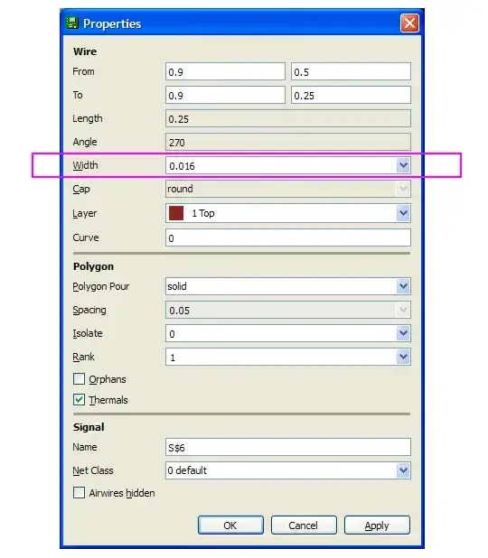
But, lets imagine you are designing for extremely high volume and want to get the absolute best price, so you are designing for 6/6 or even 8/8 rules. In that case, the best thing to do is make your design tool aware of your rules. I can't help with Eagle specifically, but any worthwhile layout tool should have settings for the space/trace design rules, and it should respect them when laying out polygons.
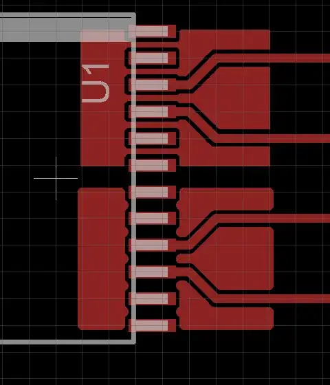
Even if your tool doesn't do this, there should be workarounds. The key thing is that polygons are built by simply serpentining a long trace back and forth to fill an area. As Nick shows, one work around is to change the width of this long trace so that it won't fit into the gaps that are causing the problem. The trade-off, as you can see in Nick's images, is that other features of the polygon, like the corners, becomes more coarse or rounded.
Another option is that most layout tools have fairly sophisticated design rule options (unfortunately if your tool is so simple that it can't understand a simple space/trace design rule, this might not be available to you). For example, you should be able to specify a specific clearance rule for polygons on the top layer and SOIC footprints. If you increase this clearance, you should be able to prevent the tool from attempting to fill the space between the pads.