-1

Schematic of the flyback

I'm working on a Flyback converter for approx. 28V/12V for 30W throughput. I'm using the IC "ADP1071-2" which provides isolation, and a lot of interesting features. I've been considering Vishay NMOSes for the switching transistor, and this being a flyback (discontinuous), most of low-Rdson MOSFETs have a higher Qg and thus heavy switch-off losses. Frequency of operation is 400 kHz.

Is there (and there may not be any practical way to do this) a way to reduce fall-time of Q1 WITHOUT adding a driver IC and without disrupting the PWM IC ? I'm looking for something that would be 5 components max.

Down here is the switch-off profile : Blue is direct current, Red is Vds and green is dissipated power.
Current, Vds and dissipated power waveforms of flyback switch-off

Harnex
  • 166
  • 8
  • When you're trying to shave nanoseconds, layout matters. Whats your circuit look like??? – Kyle B May 15 '20 at 07:44
  • @KyleB it doesn't look like anything for now, I'm still in the early design phase. What would be a good way to lay this out ? I'm planning to reduce current loops so as to reduce EMI, and that would probably put the PWM IC a little farther from the MOSFET than ideal. Is this what you're referring to ? – Harnex May 15 '20 at 07:51
  • 1
    If you want more turn-off current from the driver, you can add an extra PNP transistor to accelerate the turn-off sequence: emitter to gate, collector to ground and base to PWM driver, then diode between emitter (A) and base (K). Look at application notes on drivers, there are plenty of external circuits like Figure 13 [here](http://www.ti.com/lit/ml/slua618a/slua618a.pdf?&ts=1589529269009). – Verbal Kint May 15 '20 at 07:55
  • 1
    The [FET datasheet](http://www.vishay.com/docs/75348/sir692dp.pdf) indicates that you are getting perhaps better switching time than you might expect. Knowing what the gate voltage and current waveforms are like would help decide on whether more drive would help. A pushpull gate driver can be achieved with a small and NPN and PNP bipolar pair.(2 components). – Russell McMahon May 15 '20 at 08:39
  • Is there an echo in here? – Andy aka May 15 '20 at 09:35
  • @VerbalKint thank you for the AN, I will check this out, this looks like a good way to achieve what I want to do. – Harnex May 15 '20 at 10:03
  • Avec plaisir, I can see the comments on your curves are in French : ) Depending on the amount of charges to be evacuated, look at the Zetex (now diode Inc.) ZTX751 which could do the job well. – Verbal Kint May 15 '20 at 11:53
  • @Andyaka Did someone (else) mention measuring gate waveforms, gate waveforms gate wave .... ? – Russell McMahon May 15 '20 at 11:54
  • I didn't say everything was echoing. – Andy aka May 15 '20 at 11:56
  • The second circuit [here](https://electronics.stackexchange.com/a/140105/3288) is an example of the two-bipolars and nothing else gate driver circuit I mentioned. – Russell McMahon May 15 '20 at 11:59
  • 1
    @Andyaka You may find that there are fewer echoes than your brain suggests. Or, if not, there may be fewer echoes than your brain suggests :-). – Russell McMahon May 15 '20 at 12:01

2 Answers2

0

I'm using the IC \$\color{red}{\text{"ADP1071-2"}}\$ which provides isolation, and a lot of interesting features. I've been considering Vishay NMOSes for the switching transistor, and this being a flyback \$\color{red}{\text{(discontinuous)}}\$

The ADP1071-2 does not operate in \$\color{red}{\text{discontinuous}}\$ mode: -

enter image description here

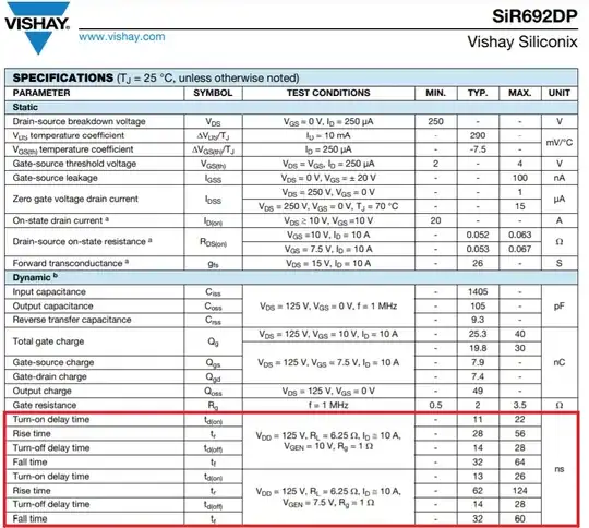
Regarding the SiR692DP MOSFET, you might have problems reducing the turn-off or turn-on times: -

enter image description here

By the looks of your diagram you already have 30 ns fall time on the current and that looks about as good as you are going to get from this device. Having said that, you need to examine the data sheet and assure your self that the figures quoted are applicable to your specific design.

Looking at the data sheet and considering the MOSFET's output capacitance (\$C_{OSS}\$), I think at least 50% of the timing problem arises from this: -

enter image description here

  • When the device first turns off, \$V_{DS}\$ is around 0 volts and \$C_{OSS}\$ is over 3 nF
  • As \$V_{DS}\$ rises, \$C_{OSS}\$ does drop and probably accounts for 50% of the problem thereafter.
Andy aka
  • 434,556
  • 28
  • 351
  • 777
  • I've looked at the ADP1071's theory of operation, and this restriction is only based off of the way the synchronous rectification works, which I do not use. Since the SR allows no dead time, I can't work in a regular discontinuous fashion. Regarding the MOSFET, I know what I'm getting is within specs, but I was wondering if there was a way to decrease only the turn-off time. – Harnex May 15 '20 at 07:58
  • Does not compute: *Since the SR allows no dead time, I can't work in a regular discontinuous fashion.* - you say in your question that you are using discontinuous mode. Can you properly explain your philosophy? Not using the sync rectifiers doesn't mean you are not in CCM. – Andy aka May 15 '20 at 08:33
  • My coupled inductor inductance value dictates that I'm in DCM with a 27V input (DCM up until 16V approx.) for 2.5A/12V output. What I'm saying is, DCM means there is almost always a dead time (if it's a fixed-frequency design, which it is). The way the ADP works is it turns off SR only when it is about to turn on the primary FET. This doesn't allow dead time, because after the energy is transfered from the inductor to the load, the process starts to reverse and energy is transfered from the load to the inductor, until SR turns off. – Harnex May 15 '20 at 09:56
  • Fact1 the data sheet says on the front page that the ADP1071-2 is forced CCM - this means it uses CCM irrespective of whether you use synchronous rectifiers or not (Fact2). You don't require synchronous rectifiers to operate a flyback design in CCM (fact 3). So, I don't really compute what you are saying plus the speed isn't going to improve without changing the MOSFET. If you want DCM then why are you not using the "01" version of the ADP1071? – Andy aka May 15 '20 at 10:04
  • 1.Difference between the two is LLM mode which is exclusive to ADP1071-1. These are equivalent if you don't use LLM. Current mode PWMs cannot enforce CCM/DCM. It works in exactly the same way, detecting peak current. 2.Yes I know that. That's not what I was suggesting. I know how my design works, but you're welcome to put these values into TI's Power Stage Designer to check out the waveforms for yourself. 3. My frequency and current range makes it so that I really have to compromise between conduction and switching losses. I'm looking for a way to pick a low Rdson FET and reduce falltime. – Harnex May 15 '20 at 10:17
  • as I can't do the other way around : picking a low gate charge FET with high Rdson will make it impossible to reduce conduction losses. – Harnex May 15 '20 at 10:18
  • OK - I see you can't use the 01 version for your voltage range anyway. One thing about this site is something called "shopping questions" - covered [here](https://electronics.stackexchange.com/help/on-topic). Please read that - it's not long but the bottom line is don't ask for shopping recommendations. – Andy aka May 15 '20 at 10:23
  • Once again, I'm not looking for a FET suggestion, I'm looking for a design topology allowing me to pull down the MOS gate. Some were shared in the comment section of the OP. Thanks for your time anyway. – Harnex May 15 '20 at 10:26
0

Beside using a dedicated driver, one easy way to reduce the turn-off sequence is to add a small PNP transistor which will help accelerating the transition and limit the switching losses. Such a solution is described in the classical application note written by Monsieur Balogh and shows the PNP in action:

enter image description here

Look for a transistor which can handle a sufficiently-high current for this job. If a 2N2907 can certainly make it for a low-\$Q_G\$ transistor, a stronger device should be considered for large-\$Q_G\$ MOSFETs. The ZTX751 could be a potential candidate.

Just one final point, a potentially-adverse reverse-bias stress of the base-emitter junction of the transistor can be underlined by some QA department. That is the reason why, sometime, a base resistance is added. Something worth considering for a high-volume design.

Verbal Kint
  • 20,420
  • 1
  • 16
  • 50