2

Hello I would like to design protection for my N and P channel MOSFETS against inductive load. According to this article, Their IC is best but it cannot hanndle my application so i have to use the next best which is to use a TVS setup as to only a free wheeling diode

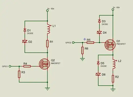
I will be using the NMOS BUK9K134 and the PMOS FDS8935, My load will be 5v to 60v DC at maximum 2A (befor efuse trips), circuit is in this configuration:

enter image description here

First of all Is the configuration correct? I dont get why you need a clamp on the gate of the PMOS. Next is how do i select the values for diode and zener diode? what would their power rating be?
DrakeJest
  • 699
  • 6
  • 24
  • I am also making a similar circuit, we are even using the same PMOS chip. It would seem that varius articles such as [this](https://www.te.com/commerce/DocumentDelivery/DDEController?Action=srchrtrv&DocNm=13C3264_AppNote&DocType=CS&DocLang=EN) also agree that a back to back diode is the choice to use which also can prolong the lifespan of the coils. – Jake quin Apr 24 '20 at 02:16
  • A answer to a question i asked have bits of info [check it out](https://electronics.stackexchange.com/questions/494826/what-should-i-look-out-for-when-driving-high-power-relays-with-mosfets/494829?noredirect=1#comment1259856_494829). But that is also as far i have gone – Jake quin Apr 24 '20 at 02:48
  • 1
    @Jakequin thanks i will have a look into it – DrakeJest Apr 24 '20 at 02:48

2 Answers2

1

First of all Is the configuration correct? I don't get why you need a clamp on the gate of the PMOS.

Bot of your configurations are correct. For the \$p\$-channel MOSFET circuit you need the gate clamp because, when the input signal \$\mathrm{GPIO2}\$ is zero, \$V_{GS_{Q_1}}\$ can range from \$-5\$ to \$-60\mathrm{V}\$ and this is clearly unacceptable.

Next is how do I select the values for diode and zener diode? what would their power rating be?

I'll show you the calculation for the \$n\$-channel MOSFET circuit as for the \$p\$-channel one the method is entirely analogous.

  1. First, let's calculate the drain ON current, i.e. the current flowing when the MOSFET is fully conducting: $$ I_{DQ_{2_\mathrm{ON}}}\simeq\frac{V_{DD}}{R_1+R_{DS_{Q_2}}} $$ where \$V_{DD}\$ is the power supply voltage, ranging from \$5\$ to \$60\mathrm{V}\$ as stated in your schematics, while \$R_{DS_{Q_2}}\$ is the drain-source ON resistance of the MOSFET \$Q_2\$.
  2. The current \$I_{DQ_{2_\mathrm{ON}}}\$ is the initial current \$I_{0_{L_1}}\$ which flows in the \$L_1\$ inductor when \$Q_2\$ is turned OFF, and assuming that the MOSFET is able to do so in negligible time, by applying the Kirchhoff current law to the drain node of \$Q_2\$ we have that $$ I_{A_{D_1}}=I_{A_{D_2}}=I_{0_{L_1}}=I_{DQ_{2_\mathrm{ON}}}\;\text{ at }\;t=0_+ $$
  3. Then you should choose a freewheel diode and a Zener diode in order that the following maximum power relationship are always fulfilled $$ \begin{split} I_{DQ_{2_\mathrm{ON}}} V_{A_{D_1}}&\le P_{D_{1_\max}}\\ I_{DQ_{2_\mathrm{ON}}} V_{Z_{D_2}}&\le P_{D_{2_\max}} \end{split} $$ where \$V_{A_{D_1}}\$ is the anode voltage of the \$D_1\$ diode when its anode current is \$I_{A_1}=I_{DQ_{2_\mathrm{ON}}}\$ and \$V_{Z_{D_2}}\$ is the nominal Zener voltage of the Zener diode \$D_2\$.
Daniele Tampieri
  • 3,161
  • 4
  • 14
  • 29
  • Thank you for the answer i always like that formulas are given in an answer in the future i can easily come back to it – DrakeJest Apr 24 '20 at 05:56
  • First problem is if R1 is not present ( because for situations like the interchangable coils they also have different resistances) should i assume it 0 ? or its better to assume a high value ' – DrakeJest Apr 24 '20 at 05:58
  • @DrakeJest \$R_1\$ can be removed as a resistor i.e. as a part. However, there is always a series resistance given by the winding resistance of the inductor \$L_1\$. This is the reason for which I used the \$\simeq\$ in the formula for the ON drain current: if the resistor is absent, you should try to estimate the minimum winding resistance of the various \$L_1\$ you can mount, since you can assume \$R_1\$ to be zero, but this would probably lead to an oversize of \$D_1\$ and \$D_2\$. – Daniele Tampieri Apr 24 '20 at 06:08
  • i guess i dont mind it being oversized since it cant hurt to go higher than lower, let me try to solve using your formula, the typical resistance on the PMOS is 176mOhm @ 5v (my GPIO voltage) for my min voltage 5v; Idq2on = 5/0.176 = 28.41A( thats a lot) and 60/0.176 = 340.41A – DrakeJest Apr 24 '20 at 06:23
  • 2
    @DrakeJest when selecting diodes on the store in their data sheets they dont usually write the power that the diode can handle. What i think are the important parameters are the Max continuos/Pulsed current, Max Reverse Voltage. I myself dont know how to choose them for the application unfortunatly. but let me just tell you that a 30A - 300A diodes comes in huge packages – Jake quin Apr 24 '20 at 06:27
0

Connect R6 to the rail. Otherwise the Pfet is always on.

analogsystemsrf
  • 33,703
  • 2
  • 18
  • 46
  • That would still not resolve it, if R6 was moved between the gate and the + rail, that may work, in addition I would suggest using an NPN transistor to switch on the Pfet a bit harder, you might want to expand you answer. – Reroute Apr 24 '20 at 12:19
  • I actually want the PFet to be defaulty ON in my application. Im a bit confused though if i use a PFET is double clamping (the gate and the coil) really necessary? – DrakeJest Apr 24 '20 at 12:42
  • @Reroute May i ask why would i still use a transistor to switch the mosfet? i mean the mosfet i have chosen are logic level driven mosfet at 5v they are pretty much fully on, also if i also use the + rail to switch the mosfet will be surpass its maximum gate voltage if the supply is 20V and higher – DrakeJest Apr 24 '20 at 12:45