10

A colleague and I had a discussion and a disagreement about the different ways high speed signals can be length-matched. We were going with an example of a DDR3 layout.

Example routing

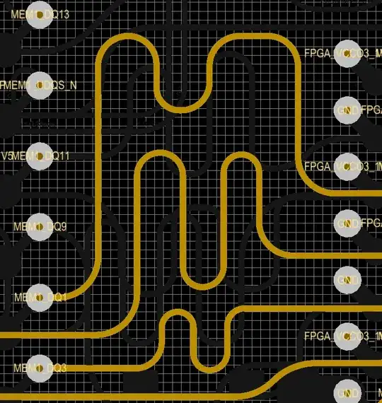
All the signals in the picture below are DDR3 data signals, so they are very fast. To give you a sense of the scale, the entire X axis of the picture is 5.3mm and the Y axis is 5.8mm.

My argument was that, length matching done as in the middle trace in the picture can be detrimental to signal integrity, although this is just based on an intuition, I have no data to back this up. The traces in the top and bottom sides of the picture should have better signal quality, I thought, but again, I have no data to back this claim.

I would like to hear your opinions and especially experiences about this. Is there a rule of thumb for length matching high speed traces?

Unfortunately, I could not simulate this in our SI tool because it is having a difficulty in importing the IBIS model for the FPGA that we're using. If I can do that, I'll report back.

Fizz
  • 14,355
  • 2
  • 43
  • 97
SomethingBetter
  • 2,260
  • 7
  • 26
  • 33
  • 2
    I don't see what's different about the middle trace from the "top" and "bottom" traces (unless you mean the really bottommost trace). What feature exactly is it that you're concerned about? – The Photon Nov 18 '12 at 17:52
  • The "aspect ratio" if you will. I mean, the fact that the length matching causes the same signal trace to end up in parallel with itself for a longer interval, increasing the probability of crosstalk. – SomethingBetter Nov 18 '12 at 17:57

4 Answers4

3

I don't work with DDR memory, so I'll assume there's no on-chip deskewing available, and length matching is in fact required. If the chips themselves are able to do the de-skewing, of course you should use that feature rather than extend the traces to do length matching.

But given that length matching is required, it looks like everything you're doing is done as well as it can be. Mainly because, 1, you're actually doing the length matching, and 2, you're using arcs rather than 90 or 45 degree bends.

In your comment, you mention your concern that the serpentine shape puts the trace in parallel with itself. That's a reasonable concern, but there's not much you can do about it. Certainly I wouldn't suggest moving the two chips farther apart to enable separating the traces further apart --- and anyway you probably have a board space limitation to prevent it. Given the spacing between traces looks like 4x or more the trace width, I wouldn't expect this to cause a serious problem.

Of course a simulation with HyperLynx or other good SI tool is a better way to get a definitive answer. You should be able to simulate this particular issue without having models for your actual chips.

One thing you haven't shown is your board stack-up. Without a good simulation and good knowledge of your materials, its not obvious that the propagation velocity on the inner layers is equal to the velocity on the outer layers (it probably isn't), and that strictly length matching between the layers is the right thing to do. Even if you have accounted for that, you can expect some variation in materials to cause mismatch between trace delays on different layers.

The Photon
  • 126,425
  • 3
  • 159
  • 304
2

Your intuition is correct, depending on edge speed and how close those serpentine paths are you can cause your self problems. They absolutely will couple to each other like you're wondering. In fact if it's tight enough the high frequency component may just couple straight through the S curves like they aren't even there.

The question then becomes will that coupling be a problem in your application. They look far enough apart in that picture for DDR3 but it's hard to tell. Of course simulation of the path would always be best, but I know we don't all always have access to expensive tools when we need them :)

You seem to be on the right path though. Here's Johnson talking a little more about it.

Some Hardware Guy
  • 15,815
  • 1
  • 31
  • 44
1

For microwave signals you want to avoid sharp corners on tracks to avoid complex return loss effects. This is why they are all smooth lines. Also to improve signal integrity , you want a ground plane. Then there is less sensitivity to layout differences and crosstalk as long as track length is matched. Trace thickness needs to be calculated based on desired impedance for improved TDR response and reflection coeficient.

You layout software ought to generate equal line length on demand.

enter image description here

Many more DDR3 layout considerations here are offered.

Tony Stewart EE75
  • 1
  • 3
  • 54
  • 182
0

For DDR3 any of those traces should be fine. The middle one could have more coupling compared to other two traces. But if you check commercial DDR3 layout designs, or even DDR4 layouts, you may notice they have tighter clearances than this and more serpentines. You may get an idea from reference layout of the particular processor chip if such layout is available.