There is already a similar question, however the design procedure is still misssing there. Now to your questions:
I can't really find characteristic curves for transistors on datasheets which makes it difficult.
Although there is no output characteristic curve in the datasheet, you can find specific biasing points which might already fulfill your needs. e.g: If you want to have a 10mA collector current, your gain is more-or-less 75A/A and from there you can work out the rest.
Another alternative, is to run a Spice simulation with models made available by the manufacturer:

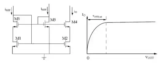
Say I have biased such that VC = 5 V and IC = 10 mA. If I then connect my load in parallel from the VC node how can I determine the current?
The idea here (not always the case) is that you want to have the collector voltage half the supply voltage. why? If the Vc = Vcc /2 it means that the collector voltage has more headroom to swing up and down without clamping the amplified signal. The drawback of it is that this class A amplifier burns current even if it not amplifying any signal. This collector current is going to be used to determine the bias point (Vc = Vcc/2), and theoretically you should driving your load directly with this current, otherwise you would move the transistor to another operating point (meaning, collector voltage would change) e.g.
- Connect a load to the collector output
- The load will draw some current
- The total current is upper limited by the collector resistor
- Current flowing into the collector reduces
- Operating point changes
- Amplified signal might be distorted
How to solve this probblem? What you usually do, is to connect a high impedance load which can deliver the current required by the load. So, at the same time you do not disturb the operating point of your amplifier, and drive a low impedance load (loudspeaker). This is accomplished by adding a buffer to the output of your amplifier as shown in the link above and here:


