Well, we have the following circuit:
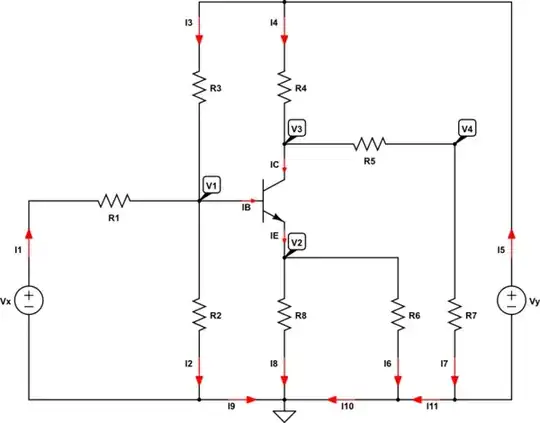
simulate this circuit – Schematic created using CircuitLab
When analyzing a transistor we need to use the following relations:
- $$\text{I}_\text{E}=\text{I}_\text{B}+\text{I}_\text{C}\tag1$$
- Transistor gain \$\beta\$:
$$\beta=\frac{\text{I}_\text{C}}{\text{I}_\text{B}}\tag2$$
- Emitter voltage:
$$\text{V}_\text{E}=\text{V}_1-\text{V}_2\tag3$$
When we use and apply KCL, we can write the following set of equations:
$$
\begin{cases}
\text{I}_2=\text{I}_1+\text{I}_9\\
\\
0=\text{I}_8+\text{I}_9+\text{I}_{10}\\
\\
\text{I}_{10}=\text{I}_6+\text{I}_{11}\\
\\
\text{I}_7=\text{I}_5+\text{I}_{11}\\
\\
\text{I}_\text{E}=\text{I}_6+\text{I}_8\\
\\
\text{I}_1+\text{I}_3=\text{I}_\text{B}+\text{I}_2\\
\\
\text{I}_4=\text{I}_\text{C}+\text{I}_7\\
\\
\text{I}_5=\text{I}_3+\text{I}_4
\end{cases}\tag4
$$
When we use and apply Ohm's law, we can write the following set of equations:
$$
\begin{cases}
\text{I}_1=\frac{\text{V}_\text{x}-\text{V}_1}{\text{R}_1}\\
\\
\text{I}_2=\frac{\text{V}_1}{\text{R}_2}\\
\\
\text{I}_3=\frac{\text{V}_\text{y}-\text{V}_1}{\text{R}_3}\\
\\
\text{I}_4=\frac{\text{V}_\text{y}-\text{V}_3}{\text{R}_4}\\
\\
\text{I}_5=\frac{\text{V}_3-\text{V}_4}{\text{R}_5}\\
\\
\text{I}_6=\frac{\text{V}_2}{\text{R}_6}\\
\\
\text{I}_7=\frac{\text{V}_4}{\text{R}_7}\\
\\
\text{I}_8=\frac{\text{V}_2}{\text{R}_8}
\end{cases}\tag5
$$
Solving these systems of equations is possible, I used Mathematica:
In[1]:=FullSimplify[
 Solve[{VE == V1 - V2, β == IC/IB, IE == IB + IC, I2 == I1 + I9,
    0 == I8 + I9 + I10, I10 == I6 + I11, I7 == I5 + I11,
   IE == I6 + I8, I1 + I3 == IB + I2, I4 == IC + I7, I5 == I3 + I4,
   I1 == (Vx - V1)/R1, I2 == (V1)/R2, I3 == (Vy - V1)/R3,
   I4 == (Vy - V3)/R4, I5 == (V3 - V4)/R5, I6 == (V2)/R6,
   I7 == (V4)/R7, I8 == (V2)/R8}, {IB, IC, IE, I1, I2, I3, I4, I5, I6,
    I7, I8, I9, I10, I11, V1, V2, V3, V4}]]

Out[1]={{IB -> -(((R6 + R8) (R1 (R2 + R3) VE + R2 R3 (VE - Vx) -
          R1 R2 Vy))/(R2 R3 R6 R8 (1 + β) +
        R1 (R2 R3 (R6 + R8) + R2 R6 R8 (1 + β) +
           R3 R6 R8 (1 + β)))),
  IC -> -(((R6 + R8) (R1 (R2 + R3) VE + R2 R3 (VE - Vx) -
          R1 R2 Vy) β)/(R2 R3 R6 R8 (1 + β) +
        R1 (R2 R3 (R6 + R8) + R2 R6 R8 (1 + β) +
           R3 R6 R8 (1 + β)))),
  IE -> -(((R6 + R8) (R1 (R2 + R3) VE + R2 R3 (VE - Vx) -
          R1 R2 Vy) (1 + β))/(R2 R3 R6 R8 (1 + β) +
        R1 (R2 R3 (R6 + R8) + R2 R6 R8 (1 + β) +
           R3 R6 R8 (1 + β)))),
  I1 -> (-R2 R3 (R6 + R8) (VE - Vx) + R3 R6 R8 Vx (1 + β) +
      R2 R6 R8 (Vx - Vy) (1 + β))/(R2 R3 R6 R8 (1 + β) +
      R1 (R2 R3 (R6 + R8) + R2 R6 R8 (1 + β) +
         R3 R6 R8 (1 + β))),
  I2 -> (R1 R3 (R6 + R8) VE + R3 R6 R8 Vx (1 + β) +
      R1 R6 R8 Vy (1 + β))/(R2 R3 R6 R8 (1 + β) +
      R1 (R2 R3 (R6 + R8) + R2 R6 R8 (1 + β) +
         R3 R6 R8 (1 + β))),
  I3 -> (-R1 R2 (R6 + R8) (VE - Vy) -
      R2 R6 R8 (Vx - Vy) (1 + β) +
      R1 R6 R8 Vy (1 + β))/(R2 R3 R6 R8 (1 + β) +
      R1 (R2 R3 (R6 + R8) + R2 R6 R8 (1 + β) +
         R3 R6 R8 (1 + β))),
  I4 -> (R2 R6 R8 (R5 (Vx - Vy) + R3 Vy) +
      R2 (-R3 R7 (R6 + R8) (VE - Vx) + R5 R6 R8 (Vx - Vy) +
         R3 R6 R8 Vy) β +
      R1 ((R3 -
            R5) R6 R8 Vy - (R3 R7 (R6 + R8) VE + (-R3 +
               R5) R6 R8 Vy) β +
         R2 (R5 (R6 + R8) (VE - Vy) + R3 R6 Vy + (R3 + R6) R8 Vy -
            R7 (R6 + R8) VE β +
            R6 R7 Vy β + (R6 + R7) R8 Vy β)))/((R4 + R5 +
        R7) (R2 R3 R6 R8 (1 + β) +
        R1 (R2 R3 (R6 + R8) + R2 R6 R8 (1 + β) +
           R3 R6 R8 (1 + β)))),
  I5 -> (R2 R6 R8 (-(R4 + R7) Vx + (R3 + R4 + R7) Vy) +
      R2 (-R3 R7 (R6 + R8) (VE - Vx) + R3 R6 R8 Vy +
         R6 (R4 + R7) R8 (-Vx + Vy)) β +
      R1 (R6 (R3 + R4 + R7) R8 Vy - R3 R7 (R6 + R8) VE β +
         R6 (R3 + R4 + R7) R8 Vy β +
         R2 (-R4 (R6 + R8) (VE - Vy) + R3 R6 Vy + R3 R8 Vy -
            R7 R8 (VE - Vy) (1 + β) -
            R6 (R7 VE - (R7 + R8) Vy) (1 + β))))/((R4 + R5 +
        R7) (R2 R3 R6 R8 (1 + β) +
        R1 (R2 R3 (R6 + R8) + R2 R6 R8 (1 + β) +
           R3 R6 R8 (1 + β)))),
  I6 -> -((R8 (R1 (R2 + R3) VE + R2 R3 (VE - Vx) -
          R1 R2 Vy) (1 + β))/(R2 R3 R6 R8 (1 + β) +
        R1 (R2 R3 (R6 + R8) + R2 R6 R8 (1 + β) +
           R3 R6 R8 (1 + β)))),
  I7 -> (R2 R6 R8 (R5 (Vx - Vy) + R3 Vy) +
      R2 (R3 (R4 + R5) (R6 + R8) (VE - Vx) + R5 R6 R8 (Vx - Vy) +
         R3 R6 R8 Vy) β +
      R1 (R3 R6 R8 Vy +
         R3 ((R4 + R5) (R6 + R8) VE + R6 R8 Vy) β -
         R5 R6 R8 Vy (1 + β) +
         R2 (R6 R8 Vy + R3 (R6 + R8) Vy +
            R4 (R6 + R8) (VE - Vy) β + R6 R8 Vy β +
            R5 (R6 + R8) (VE - Vy) (1 + β))))/((R4 + R5 +
        R7) (R2 R3 R6 R8 (1 + β) +
        R1 (R2 R3 (R6 + R8) + R2 R6 R8 (1 + β) +
           R3 R6 R8 (1 + β)))),
  I8 -> -((R6 (R1 (R2 + R3) VE + R2 R3 (VE - Vx) -
          R1 R2 Vy) (1 + β))/(R2 R3 R6 R8 (1 + β) +
        R1 (R2 R3 (R6 + R8) + R2 R6 R8 (1 + β) +
           R3 R6 R8 (1 + β)))),
  I9 -> (R1 R3 (R6 + R8) VE + R2 R3 (R6 + R8) (VE - Vx) -
      R2 R6 R8 (Vx - Vy) (1 + β) +
      R1 R6 R8 Vy (1 + β))/(R2 R3 R6 R8 (1 + β) +
      R1 (R2 R3 (R6 + R8) + R2 R6 R8 (1 + β) +
         R3 R6 R8 (1 + β))),
  I10 -> (R1 R2 R6 (VE - Vy) (1 + β) +
      R2 R6 R8 (Vx - Vy) (1 + β) - R1 R6 R8 Vy (1 + β) -
      R2 R3 (VE - Vx) (R8 - R6 β) +
      R1 R3 VE (-R8 + R6 β))/(R2 R3 R6 R8 (1 + β) +
      R1 (R2 R3 (R6 + R8) + R2 R6 R8 (1 + β) +
         R3 R6 R8 (1 + β))),
  I11 -> (R2 R6 R8 (Vx - Vy) +
      R2 (R3 (R6 + R8) (VE - Vx) + R6 R8 (Vx - Vy)) β +
      R1 (R3 R6 VE β + R3 R8 VE β +
         R2 (R6 + R8) (VE - Vy) (1 + β) -
         R6 R8 Vy (1 + β)))/(R2 R3 R6 R8 (1 + β) +
      R1 (R2 R3 (R6 + R8) + R2 R6 R8 (1 + β) +
         R3 R6 R8 (1 + β))),
  V1 -> (R2 (R1 R3 (R6 + R8) VE + R3 R6 R8 Vx (1 + β) +
        R1 R6 R8 Vy (1 + β)))/(R2 R3 R6 R8 (1 + β) +
      R1 (R2 R3 (R6 + R8) + R2 R6 R8 (1 + β) +
         R3 R6 R8 (1 + β))),
  V2 -> -((R6 R8 (R1 (R2 + R3) VE + R2 R3 (VE - Vx) -
          R1 R2 Vy) (1 + β))/(R2 R3 R6 R8 (1 + β) +
        R1 (R2 R3 (R6 + R8) + R2 R6 R8 (1 + β) +
           R3 R6 R8 (1 + β)))),
  V3 -> (R2 (R3 R4 R7 (R6 + R8) (VE - Vx) β -
         R4 R5 R6 R8 (Vx - Vy) (1 + β) +
         R3 R6 (R5 + R7) R8 Vy (1 + β)) +
      R1 (R3 R6 (R5 + R7) R8 Vy + R3 R4 R7 (R6 + R8) VE β +
         R3 R6 (R5 + R7) R8 Vy β +
         R4 R5 R6 R8 Vy (1 + β) -
         R2 R4 (R6 + R8) (VE - Vy) (R5 - R7 β) +
         R2 (R5 + R7) Vy (R3 (R6 + R8) + R6 R8 (1 + β))))/((R4 +
         R5 + R7) (R2 R3 R6 R8 (1 + β) +
        R1 (R2 R3 (R6 + R8) + R2 R6 R8 (1 + β) +
           R3 R6 R8 (1 + β)))),
  V4 -> (R7 (R2 R6 R8 (R5 (Vx - Vy) + R3 Vy) +
        R2 (R3 (R4 + R5) (R6 + R8) (VE - Vx) + R5 R6 R8 (Vx - Vy) +
           R3 R6 R8 Vy) β +
        R1 (R3 R6 R8 Vy +
           R3 ((R4 + R5) (R6 + R8) VE + R6 R8 Vy) β -
           R5 R6 R8 Vy (1 + β) +
           R2 (R6 R8 Vy + R3 (R6 + R8) Vy +
              R4 (R6 + R8) (VE - Vy) β + R6 R8 Vy β +
              R5 (R6 + R8) (VE - Vy) (1 + β)))))/((R4 + R5 +
        R7) (R2 R3 R6 R8 (1 + β) +
        R1 (R2 R3 (R6 + R8) + R2 R6 R8 (1 + β) +
           R3 R6 R8 (1 + β))))}}
Now, I've a question for you: what do you mean by 'The lower cutoff frequency of CE is to be found'? The lower cutoff frequency of a component is a weird question.