First off:
- This is for a one-off (or two-off) hobby project, nothing more serious. If this were a commercial design, I would go 4-layer at once (though I wouldn't be designing such a project in the first place).
- Going 4-layer is acceptable only if TRULY necessary; such boards cost at least twice as much in these quantities, and the 2-layer PCB still costs more than the components combined.
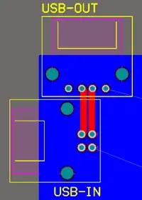
- The goal is to pass the USB 2.0 signal, mostly unharmed, between two connectors (USB-B to USB-A, both female), nothing more; my PCB does not actually use the signal.
(If these points moves the post into "too narrow" territory, feel free to ignore them :-)
So, the question is: is this possible, with acceptable results? The main goal is, of course, to allow High-Speed (480 Mbit/s) communications.
According to the USB specification, the differential pair should have a differential impedance of 90 ohm, and a to-ground characteristic impedance of 30 ohm. However, USB appears to tolerate a fair bit of abuse; an SMSC app note (PDF) where they discuss 2-layer USB 2.0 PCB layout mentions that the single-ended impedance isn't as critical as the differential, and that a "45 to 80 ohm" range is acceptable.
The board specs are 1 oz copper, with 63 mil FR-4 in between.
According to a few impedance calculators, such as this one (which, unless I misunderstand something, doesn't display the single-ended impedance as well), it appears that 50 mil traces with 10 mil spacing gives ~90 ohm differential and ~80 ohm Z0.
(Those values are from the Saturn PCB Toolkit calculator which is free, but requires download.)
The traces would be on the order of 3 inches long, and likely go in an upside-down U shape to go near the board edges, so that I have space to route everything else (sub-MHz signals only) without breaking the ground plane under the USB traces.
I do of course realize that the entire endeavor is a bit insane; however, again, it's for a hobby board, and it appears to have been done by serious companies as well.
High-speed is really still a bit beyond me, but the rest of the project is simple; I just need to get this signal across the PCB and everything else is a piece of cake.
If you missed it, the main question is: is this possible, with acceptable results?
If there are better 2-layer routing methods (for example, this short article uses coplanar waveguide routing for this purpose), please do tell. I can't find much information (that is both detailed and understandable, but with no details or equation/calculator mentions) about this at all.
 (as posted by OP).