-1

I am building a step up transformer for an output of 100 kV, 50 mA, at 50 kHz.

schematic

simulate this circuit – Schematic created using CircuitLab

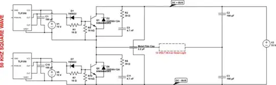
For that I have planned to use a half bridge circuit with a ferrite transformer. However to test the circuit I am putting 30 V DC across a half bridge input. I am using a TLP350 as a Gate driver. I am using 10 Ω resistor as a gate turn on resistance, and a 1N5822 as a turn off diode for gate driver.

Lower side IGBT gate voltage

This is my lower side IGBT gate voltage, the probe directly connected at IGBT legs. 15 V. The probe is in 10X mode...

Half bridge output

This is my half bridge output, load is a 60 Watt 12 Volt car headlight.

Voltage spike/overshoot at the leg of lower side IGBT

This is my issue, a voltage spike/overshoot at the leg of lower side IGBT. Probe is connected in emitter and collector pin. Collector pin referenced to emitter. This waveform taken without the snubber circuits.

My question is how I can reduce the spike at the IGBT's collector emitter pin?

Test setup

This is my test setup for now. I have a 2 µf, 2 kV snubber cap close to half bridge IGBTs. 10 kΩ resistor connected in gate and emitter at both IGBT to reduce accidental turn on. I am using IHW40N65R5 IGBT with DSEI60-12A diode with each IGBT.

Lower side IGBT collector emitter voltage with snubber

After I put the snubber circuit my lower side IGBT collector emitter voltage look like this, spike reduced but little ringing happening now... Is that ok? Can I power up my circuit up to high voltage DC? Like 300 Volt DC?

Greenonline
  • 2,064
  • 7
  • 23
  • 38
  • 2
    Show your circuit diagram. – Andy aka Mar 05 '20 at 14:14
  • 5
    No need to SHOUT in the title of your question. And **no circuit** means **no answer**. What is electronics about? Circuits. It eludes me why so many of you ask a question but don't include the **circuit**. *But the circuit is so common* sure but include it anyway. And is it **EXACTLY** as that "common circuit"? *Yes, but I changed...* So it is not exactly the same then. Details matter, that's why EEs use **circuit diagrams**. – Bimpelrekkie Mar 05 '20 at 14:22
  • 1
    This kind of photo, with no schematic, makes me want to sneak up behind the poster, and clap once. –  Mar 05 '20 at 14:53
  • Bad layout and bad probing. Improve both and measure again. – winny Mar 06 '20 at 10:22
  • @winny Bad Probing means You want me to shorten the Ground Loop in probe ?? And for the layout i still didn't make the pcb, Shoud i need to make pcb before testing ??? – Ehsan Habib Mar 06 '20 at 10:25
  • Correct. A pigtail is perferred. Yes, a real PCB or accept that you are probably snubbing away a layout related issue in this (I presume) prototype stage. – winny Mar 06 '20 at 10:48
  • 1
    @Bimpelrekkie, OP is a newcomer, so make them welcome. Please don't accuse them of shouting then do far worse. Cut the bold-shouting and the patronising tones, they drag the site's reputation right down. EEs treat anybody else - anybody - professionally and well, so become one of us who leads by example. – TonyM Mar 15 '20 at 10:55

1 Answers1

1

Limiting the inductance solved the issue.

Greenonline
  • 2,064
  • 7
  • 23
  • 38