Recently I'm trying to design a PCB board for an MCU. The problem is I haven't considered any noise aspects before. As I'm in a contest for new electronics product run by our university I have to think of all aspects. I have searched a lot about proper grounding, bypassing, and other noise stuff and got a little bit confused. Things that I learned:
- Bypassing caps are better to locate as close as possible to power pins of MCU
- It's very important to properly design PCB especially on digital clocked devices and frequencies above 50MHz (My MCU runs at 80 MHz)
- It's preferred to use power planes instead of power tracks (I'm using a 2 sided board)
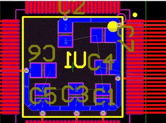
- Oscillator device should be placed as close to MCU as possible and surrounded by guard traces
- The best ground plane is the one which doesn't have traces inside
- Supply track should pass from caps first and after to power pins of MCU
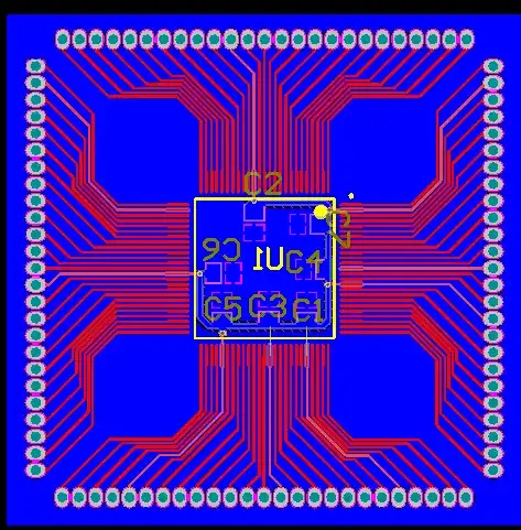
Basically it's just a breakout board or PIM board. All nets are on top side of PCB. I'm thinking of using bottom as a ground plane.
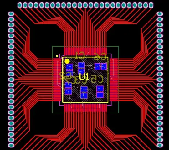
Is it a good idea to fill entire top side of PCB with copper polygon connected to + and bottom side of PCB covered with ground plane and have caps under IC connected with vias? Entire board will then act as a capacitor. I read some where that it's a good technique. By this I'll have perfect trackless ground plane on bottom side of PCB but viaed supply plane on top. And I'm not quite sure about the board acting like a cap at all. Is it a good thing to do? Why?
I have read your post, Olin. I'll try to apply local ground plane for caps.
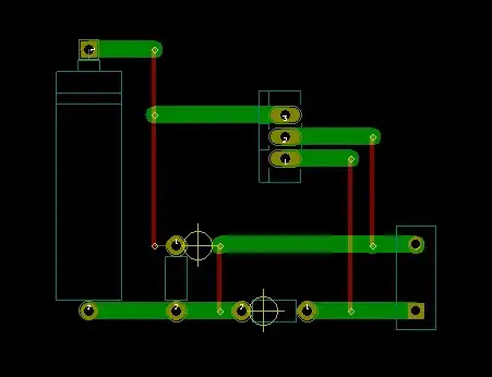
I designed something but yet not sure if its a good one.
By this I connected all VDD pins together. ( This is important for my project). But notice that power pins of MCU are connected to supply bu that track and also directly from header pins. Is it a problem? Does it couse noise and why?:)
Then I filled bottom layer with polygon connected to ground...