0

I need help understanding how to calculate tpd while static hazards are involved,

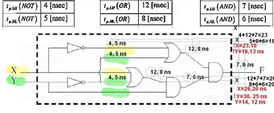
Given this circuit: (the output F is constant 0) enter image description here enter image description here I found out that if X and Y are initated to 0 and we change Y to 1 we get an hazard after the AND gates (0->1->0) which I know cause a delay in the circuit even though the output is constant.

I am having trouble understanding how to calculate the delay, for example what delay should I take into consideration (HL,LH) for the AND gates.

If I could get an explaintion and an example calculating the delay from Y to F it would help a lot (not graphic if possible).
1 Answers1

0

There are 2 paths for X and 3 paths for Y to F. You can see it both in schematic and functional equation.

\$F= (X!+Y!)\cdot ((X+Y!)\cdot Y)~~~\$ or \$F=(X!+Y!)\cdot (X\cdot Y+Y\cdot Y!))\$

If input = LH we use the inverted delay tHL for the inverter output and same polarity for OR,AND.

Thus the metastable transition times may be added up as follows. enter image description here

We see the stable F=0 but transitions for X,X! and Y,Y! may be added up to determine the worst case glitch with F=1.

A better version of this could be an edge detector and often done with edge-type logic phase-detectors used in PLL's. Can you compute the Y glitch? What about X?

FYI... The transitions are based on a fixed load capacitance like 15 pF for tLH or tHL due to the min/max R=RdsOn results in dV/dt=Vdd/T(~RC) due to PFETs used for tLH and NFETs used for tHL in addition with internal delays.

Tony Stewart EE75
  • 1
  • 3
  • 54
  • 182