I'll try and keep it to the absolute minimum needed.
The signal at the base is copied at the emitter, less by about \$700\:\text{mV}\$. So the emitter just "follows" the base around. This voltage is impressed on the emitter resistor, causing a varying emitter current that varies directly with changes in the base voltage. So \$I_\text{E}\approx \frac{V_\text{B}-700\:\text{mV}}{R_\text{E}}\$. Since \$I_\text{C}\approx I_\text{E}\$, it follows that \$V_\text{C}=V_\text{CC}-I_\text{C}\cdot R_\text{C}\$ or:
$$\begin{align*}V_\text{C}&=V_\text{CC}-\frac{V_\text{B}-700\:\text{mV}}{R_\text{E}}\cdot R_\text{C}\\\\
&=V_\text{CC}+700\:\text{mV}\cdot\frac{R_\text{C}}{R_\text{E}}-V_\text{B}\cdot\frac{R_\text{C}}{R_\text{E}}\end{align*}$$
Taking the derivative, we find:
$$\begin{align*}\text{D} \:V_\text{C}&=\text{D} \:\left[V_\text{CC}+700\:\text{mV}\cdot\frac{R_\text{C}}{R_\text{E}}-V_\text{B}\cdot\frac{R_\text{C}}{R_\text{E}}\right]\\\\
&=-\frac{R_\text{C}}{R_\text{E}}\cdot \text{D}\:V_\text{B}\\\\\therefore\\\\
\frac{\text{d}\,V_\text{C}}{\text{d}\,V_\text{B}}&=-\frac{R_\text{C}}{R_\text{E}}\end{align*}$$
So, \$A_v\approx -\frac{R_\text{C}}{R_\text{E}}\$.
With respect to your comment here below, the above does not apply to a grounded emitter, where another highly temperature dependent and highly signal dependent term arrives: \$r_e\$.
Quoting from Paul Horowitz and Winfield Hill's "The Art of Electronics," 3rd edition, page 94, right column:
"The extra voltage gain you get by using \$R_\text{E}=0\$ comes at the
expense of other properties of the amplifier. In fact, the grounded
emitter amplifier, in spite of its popularity in textbooks, should be
avoided except in circuits with over-all negative feedback."
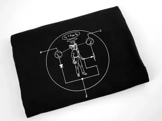
Q.E.D.