3

schematic

simulate this circuit – Schematic created using CircuitLab

I have implemented the above circuit which is supposed to amplify a negative 200kHz sinusoid to constant amplitude even if the amplitude is varied. The constant amplitude is adjusted according to the reference.

Am I missing something here? Since the amplitude of Vout still varies with the input amplitude , but doesn't vary when the Reference voltage is adjusted.

However I noticed that the overall gain of the VCA is reduced as the amplitude of the input is decreased. This remains constant if the feedback is removed.

Simon Sultana
  • 344
  • 3
  • 12
  • You appear to be rectifying to a positive output proportional to signal in; the N channel JFET will therefore be turned *on* for higher input voltages (lower resistance). Flip D1 and see what happens. – Peter Smith Nov 05 '19 at 13:51
  • 1
    Voltage going to gate of JFET is negative since OA2 is inverting the signal. Did I understand you correctly? – Simon Sultana Nov 05 '19 at 13:52
  • 1
    The input opamp has a GBW of 38 MHz, approx. 45.5 dB of open-loop forward gain at 200 kHz (datasheet chart). The circuit has a gain of 150, or 43.5 dB. This leaves only 2 dB for negative feedback to close and stabilize the loop, and that is not enough. The output impedance will be much higher than the assumed zero ohms, affecting overall gain stability, loop stability, and the loop filter (OA1 output impedance and C5) time constant. Consider breaking the input stage into two amps in series so that each one has at least 20 dB of negative feedback at the maximum frequency of interest. – AnalogKid Nov 05 '19 at 16:42

3 Answers3

3

Flip the diode around, swap the positions of the jfet and R2 and then replace the jfet with a mosfet such as a 2N7000.

Input amplitude gets larger, error out goes more positive turning on the mosfet further reducing its resistance and reducing the size of the input signal.

Connect 5k pot between +5V and -5V with its wiper to non-inverting input of OA2.

The mosfet's source is then referenced to a constant 0V and the input amplitude is small enough to not make its body diode a problem.

It will never be perfect, there must be some increase in error out in order to increase the mosfet's gate voltage.

3

The input opamp has a GBW of 38 MHz, approx. 45.5 dB of open-loop forward gain at 200 kHz (datasheet chart). The circuit has a gain of 150, or 43.5 dB. This leaves only 2 dB for negative feedback to close and stabilize the loop, and that is not enough. The output impedance will be much higher than the assumed zero ohms, affecting overall gain stability, loop stability, and the loop filter (OA1 output impedance and C5) time constant. Consider breaking the input stage into two amps in series so that each one has at least 20 dB of negative feedback at the maximum frequency of interest.

I recommend a two-stage input amplifier, with both stages non-inverting at a gain of 22 dB. The first stage is a fixed-gain amplifier/buffer to present a constant input impedance to the signal source and a constant output impedance to the voltage-variable attenuator. Then, a series resistor and shunt n-channel MOSFET (as described by James) into the second fixed-gain stage to make up the required total forward gain. The output of the second stage drives the rectifier and filter.

You don't say what the input signal voltage amplitude range is, or what the signal source output impedance is, so these parameters might change the input stage design. You also don't give any information about the AGC loop performance, such as its attack and release times for large changes in signal amplitude. These affect the detector and loop filter component values.
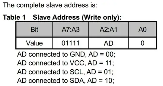
AnalogKid
  • 16,865
  • 1
  • 13
  • 25
1

Besides the mentioned observation, I like to point to the following:

In general, when using a FET as a controlled resistor, the resistance between source and drain is determined by the gate-to-source voltage. Hence, when the gate receives the control signal the source must be at a fixed potential (normally ground).

However, in your circuit, the source node is NOT connected to the virtual ground (inverting opamp input) but to the resistor R1. Therefore, the control signal is not a DC signal but swings with the input signal. You should exchange the position of R1 and the FET.

LvW
  • 24,857
  • 2
  • 23
  • 52
  • 2
    It might work better (lower distortion) if the source and gate are capacitively coupled and there is a series resistor of about 1 Mohm coming from the op-amp output to the gate. – Andy aka Nov 05 '19 at 14:49