No, you can never make sure there are no glitches in your design.
In real designs you find that glitches are caused by delays in the logic because one signal path is longer then another. You must make sure that glitches have gone by the time the signal get to the input of a register and the clock arrives. (Set-up time).
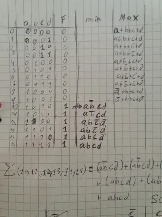
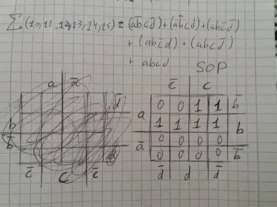
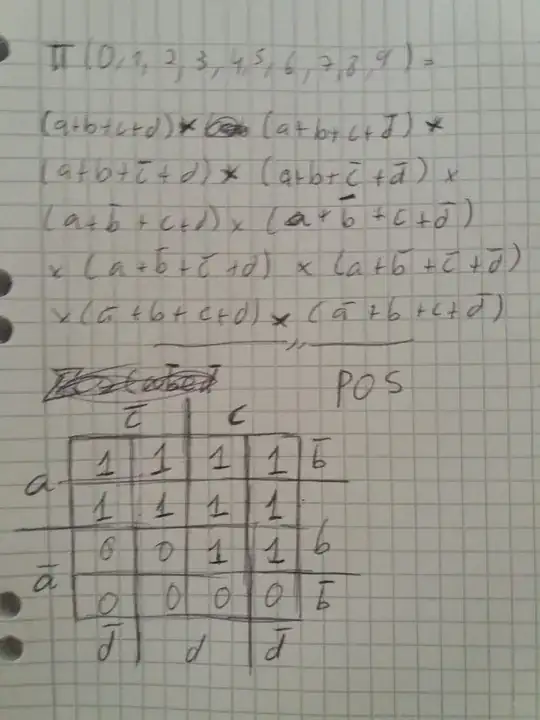
I had never heard of, lets call them "Karnaugh" glitches, and honestly to me they seem a typical 'academic' problem. To reduce a Karnaugh map you end up with AND, OR, gates and inverters. Each of these will have a different delay and then you have to add to that the delay of the output (The number of inputs to drive, plus the capacitance of the wires leading to them). Pass all that through a cloud of logic and you quickly realize that nobody can avoid glitches.
Karnaugh map are necessary for a fundamental understanding how logic works, However in in HDL design you do not make Karnaugh maps and use them to design an optimise circuits. Just this morning I answered a related question here where somebody did a lot of work to find the logic equations. You can see that the HDL solution ignores all that. What the actual logic is we leave to the synthesis tool.
I admit for the few people who design the synthesis tool, they had better know how to write programs to optimize logic. Also you might have to do some special work e.g. design a 6.4GHz serial I/O circuit. That is where the fundamentals of logic design come back and you have to calculate every gate. But 99.9% of the HDL designers know about Karnaugh maps, they can solve them (or they should be able to solve them...:-) , but they do not use them.


