Original Post
This is the circuit I think you are inquiring about:
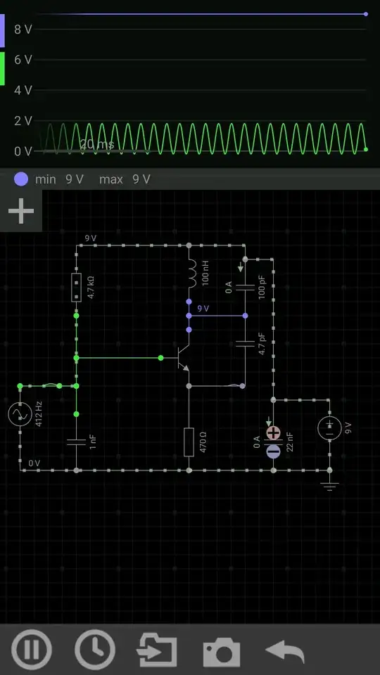
simulate this circuit – Schematic created using CircuitLab
As you can see, there are some specifications. But to be honest, not enough. No idea of \$R_\text{L}\$ or \$R_\text{S}\$ (which cannot be ignored), for example. Suppose \$R_\text{L}=3.3\:\text{k}\Omega\$? Then already you have \$\pm 1\:\text{mA pp}\$ as a compliance requirement for the output. And that's without the amplifier itself requiring anything at all to support itself. It brings up another question, too. Do you mean \$1\:\text{mA}\$ as the average current from your \$V_\text{CC}\$ supply rail? Or do you mean \$1\:\text{mA}\$ as the worst case peak value? Not specified. Yet it probably is important to know. I have no idea what the frequency is supposed to be (your schematic's AC supply says \$0\:\text{Hz}\$; but of course I'm sure that's not correct.) And no idea what the bandwidth should be, either.
Let me cut to the meat of things, though. Let's assume that you are willing to bias \$Q_1\$ in such a way that it sits just on the cusp of saturation -- say, where \$V_{\text{CE}_\text{MIN}}\approx 500-600\:\text{mV}\$. And let's also say that you are willing to have the collector voltage swing all the way to the \$V_\text{CC}\$ rail, as well. That's the absolute maximum possible collector swing. Then it follows that \$A_{v_\text{MAX}}=\frac{V_\text{CC}-V_{\text{CE}_\text{MIN}}}{V_T}\$ (assuming the usual emission coefficient of \$\eta=1\$.) At a maximum operating temperature of, say, \$50^\circ\text{ C}\$, \$V_T\approx 28\:\text{mV}\$. So this suggests \$A_{v_\text{MAX}}\approx 100\$.
That may sound good to you. But there's a problem. This only works with the BJT biased right at the very cusp of saturation. Which means that only one half-cycle of the input AC signal can be passed along. The other half-cycle is almost entirely clipped away, as it drives the BJT deeply towards saturation. And it ignores the huge distortion caused by widely varying gain for the half-cycle over which it does work.
Oh. Did I forget to mention that biasing the BJT to the very cusp of saturation, in the grounded emitter configuration you show, is quite temperature-dependent? Well, let me mention it now. That's another problem. Not much thermal stability. Even assuming you could accept its other difficulties.
I'm almost certain that's unacceptable. Which means the above calculation of \$A_{v_\text{MAX}}\$ is grossly overly optimistic. So now it seems that there may be some difficulties achieving your voltage gain goals, even temporarily ignoring the rest of the information you've failed to provide.
I have tried here to illustrate what's missing in the information you've provided and pointed you towards the singularly glaring difficulty in achieving a high voltage gain with a relatively low \$V_\text{CC}\$. I've also pointed out that there will be a great deal of distortion involved when pushing this to its limits. And I've added that all of those factors will also be temperature-dependent, which means the circuit will do different things in different seasons or areas of the world.
So you need to clarify the temperature range over which this circuit must operate, how much ripple or allowable variances there might be in \$V_\text{CC}\$, whether or not the \$1\:\text{mA}\$ current limitation is average or peak, the bandwidth required over which it must operate within these specs, the load and source impedances, etc. There's a lot missing in this. I don't see how anyone can help you without writing an entire textbook along with a set of course study materials and lesson plans.
Additions Due to Updated Question
You've added that the bandwidth is \$100\:\text{kHz}\$, the source impedance is \$5\:\text{k}\Omega\$ and the load impedance is \$100\:\text{k}\Omega\$. This still leaves out the start/end range for the frequencies of interest and it doesn't discuss what kind of distortion you can accept.
But I've something I'd like to add, as well.
For any kind of thermal stability in this general topology (by this, I'm allowing for similar circuits that include some local NFB via emitter degeneration resistors), this relationship must be true:
$$V_T\ll \frac{V_\text{CC}-V_{\text{C}_\text{Q}}}{A_v}$$
Let's assume a worst case \$V_T\approx 28\:\text{mV}\$ and your existing \$V_\text{CC}=3.3\:\text{V}\$. Let's also assume two values for \$V_{\text{C}_\text{Q}}\$: \$V_{\text{C}_\text{Q}}=2.1\:\text{V}\$ (which in a "normal" design, it might be) and \$V_{\text{C}_\text{Q}}=0.0\:\text{V}\$ (which it cannot be in any realistic/useful design.) We get the following two relations:
$$\begin{align*}
28\:\text{mV}\ll 24\:\text{mV}\tag{false}\\
28\:\text{mV}\ll 66\:\text{mV}\tag{likely false}
\end{align*}$$
I don't consider either of these to be true. The first case is obviously false on its face. The second case is false once you add in the fact that it derives from an impossible condition -- that we can set \$V_{\text{C}_\text{Q}}=0.0\:\text{V}\$ and have a useful (or buildable) amplifier. So either the condition is false by itself or else it is falsified by a false prior assumption. Either way, the whole idea loses out.
(By the way, you can derive the above relationship on your own by merely laying out the equations for \$I_\text{Q}\$, \$r_e\$, and what you'd need to do in creating some emitter degeneration to compensate for temperature.)
This leaves us with terrible compromises to consider. We can adjust \$V_{\text{C}_\text{Q}}\$ upward, thereby moving the above computed relation towards the very limits of any validity, while at the same time avoiding an out-and-out violation of it.
For example, we might say \$V_{\text{C}_\text{Q}}=1.0\:\text{V}\$ and find that \$28\:\text{mV}\ll 46\:\text{mV}\$ and figure that might be as good as we can get in this circuit. But this means that \$V_{\text{C}_\text{MIN}}=500\:\text{mV}\$ and that is already pressing the BJT into saturation and doesn't really allow us any room for emitter degeneration. But let's say we can accept \$V_{\text{CE}_\text{MIN}}=400\:\text{mV}\$ (arguably not quite yet too deeply saturated), thus allowing ourselves about \$100\:\text{mV}\$ for \$V_{\text{E}_\text{Q}}\$. Then, we find that the base biasing pair of resistors as well as \$r_\pi\$ will probably attenuate your input signal by at least 50%, destroying the goal as we try so hard to save it.
This means to me that you'd have to go to a bootstrapped design (in order to reduce the input attenuation) in order to have any chance. But you'd also have to accept other compromises (gain variation and thereby perhaps unacceptable distortion.)
If you specify more about what kind of distortion you can accept and address yourself to the above comments in my answer a little more fully, I might attempt a bootstrapped design. But only if you tell me that you can fully accept the host of compromises that such a design implies and that a bootstrapped approach doesn't otherwise violate your requirements. (It adds one resistor and one capacitor.)

