20

(This is a follow-up to this related question).

I'm interested in some feedback from people's design results/experiences with Castellated PCBs as a method of attaching one PCB to another. By Castellations, I am referring of course to Half-vias or Edge plating, as follows (both images are from Stack):

enter image description here

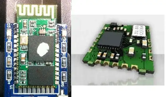
It seems to be an elegant solution, and appears to be a fairly popular form factor, especially among RF modules.

But I am concerned with (and would like comments regarding):

  • how robust the mechanical contact is
  • how reliable the electrical contact will be
  • what design methods/factors might influence the quality of the connections

E.g., one layout approach, as described by @Rocketmagnet in the earlier related question, is to place vias on the dimension outline, thus half-drilled holes act as the solderable castellations. Is this a standard/accepted method, or should a designer actually contact the PCB manufacturer and custom-design the board specifically requesting castellation addition?

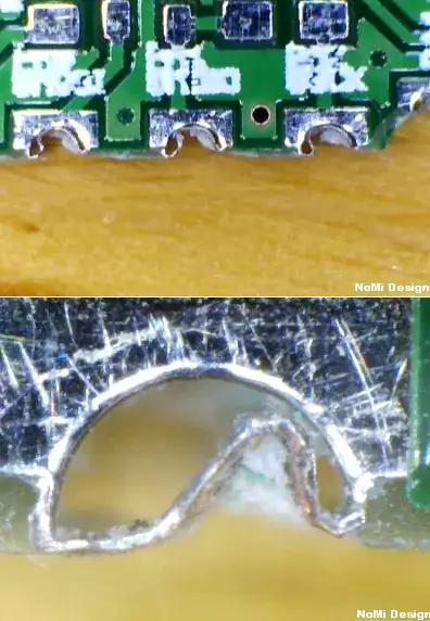
As seen in the image below, results with the half-size plated through-hole approach (from this person's blog) aren't too impressive (the page's author holds the poor milling responsible).

enter image description here

OrCa
  • 1,659
  • 4
  • 14
  • 20
  • 4
    Your pictures seem to answer the question -- putting drilled vias at the edges failed. You should always discuss unusual things like this with the PCB manufacturer first. – Jim Paris Oct 30 '12 at 15:54
  • Jim is right and should really post this as an answer instead so he can get lots of ego points. You can find PCB mfgs. that can do this without the ugly. – Mariano Alvira Oct 31 '12 at 21:14
  • @MarianoAlvira: Sounds good; I just wanted to verify the common-ness of this, and that I'm not doing anything wrong with my board layout itself which could be corrected. Have you had this done successfully with a manufacturer? The couple that I've spoken with (fairly inexpensive ones in China) said they cannot do this. – OrCa Oct 31 '12 at 21:27
  • 1
    A guy I know have Gold Phoenix do this. They called it "half-hole". And 4pcb.com has it on one of their quotation pages. Sierraprotoexpress can make anything (including 35 micron trace space !?!? ) so if they can't make it no one can.... – Mariano Alvira Oct 31 '12 at 22:16
  • @MarianoAlvira: Those recommendations are appreciated. One of you guys should go ahead and post your info above as an Answer! – OrCa Oct 31 '12 at 22:22
  • 3
    The pictures identified with the text "NoMi Design" in the lower right corner were basically plated through holes that were CNC routed through when the boards were routed free of the fabricator's process panel. When the router bit started to cut through the part of the hole being removed, the plated copper on that part of the hole wall was pushed back into the remaining part of the hole. Bisecting the hole at the end of the process is the incorrect way to do this. The proper way to form a castellation is to CNC rout somewhere between electroless copper deposition but prior to outer layer coppe – David Duross Apr 18 '13 at 12:30
  • @DavidDuross please don't use answers and comments to advertise your company, it's not an accepted practice here. But you can make an agreement for normal advertising. – clabacchio Apr 18 '13 at 15:37

2 Answers2

12

Complexity Levels (or Class levels) There are several factors that contribute to the complexity of a castellated hole. The main critical design attributes are:

  • Hole size
  • Number of holes per board
  • Single hole or multiple hole designs
  • Surface finish

Recommendations and comments When castellated features are required, it is best to use the following general rules when at all possible

  • Use the largest hole size possible
  • Use the largest Outerlayer pad possible, both top and bottom sides
  • If possible, place Innerlayer pads to anchor the hole barrel. This will also help reduce burring during the castellation process.
  • If the castellation is not used for a mechanical connection (i.e. insertion of a connector device), allow additional dimensional tolerance for the castellation opening if possible. enter image description here

courtesy of Hitech

Tony Stewart EE75
  • 1
  • 3
  • 54
  • 182
  • Just saw this answer. Useful points there. I have a board under production as of last week; let's see how it turns out. – OrCa Dec 10 '12 at 05:19
7

The pictures identified with the text "NoMi Design" in the lower right corner were basically plated through holes that were CNC routed through when the boards were routed free of the fabricator's process panel. When the router bit started to cut through the part of the hole being removed, the plated copper on that part of the hole wall was pushed back into the remaining part of the hole. Bisecting the hole at the end of the process is the incorrect way to do this. The proper way to form a castellation is to CNC rout somewhere between electroless copper deposition but prior to outer layer copper etch. Each PCB fabricator has a preference of when to bisect the plated through hole. Done properly there shall be no lifted or burred copper. There shall be no copper pushed back into the hole. An edge plated board is similarly formed.

Kortuk
  • 13,362
  • 8
  • 60
  • 85
David Duross
  • 71
  • 1
  • 1