Some quick notes:
- I'm not certain from your description what exactly you're measuring (e.g. where is scope ground, where is scope probe) in the circuit. I think 5.15 is across the drain-source of Q2 (low-side MOS)
- Your GaN FET part number returns 0 hits on Google, and looks a bit more like an EPC device instead of Infineon. Maybe an EPC2014?
- I can't really see the VDC+ trace that runs below the switching leg (bottom trace?)
- At these frequencies, your measurement technique is important. Make sure you're not seeing ringing from your oscilloscope probe connection.
- Your gate drive loop inductance may be a bit high for the speed you're switching the gates, leading to partial switching. It looks like you're on the threshold of the effect, but a heads up.
The important part of the schematic regarding the ringing you are seeing is in the loop formed through the drain-source of Q1, drain-source of Q2, and your bus capacitors (not shown in your schematic excerpts). At the switching rates, any inductive load in the uH range is effectively a constant current source. I've redrawn the relevant subcircuit below:
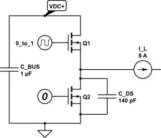
simulate this circuit – Schematic created using CircuitLab
In practice, you are getting parasitic oscillations at about 160MHz (eyeballing it, you should measure). This oscillation is based on a LC resonant circuit formed with the drain-source capacitance of Q2, and the parasitic inductance in the loop.
When you turn on Q1, the drain-source capacitance charges rapidly, forcing a current through the inductance while the output voltage rises from VDC- to VDC+. Once the voltage reaches VDC+, you have a charged inductor, and a high-Q capacitor in parallel. The result is the damped oscillations seen in your waveforms.
The waveform doesn't occur on both low-high and high-low transitions because on the high-low (Q1 turns off) transition the clamped inductive load runs up against the diode effect, which is a softer transition than the other way around. If you got a waveform with the current flowing into the switching leg, then I would expect the ringing to be on opposite waveforms.
There are two ways to reduce the ringing you see: increasing the turn-on time, and reduce the parasitic inductance in the Q1, Q2, Cbus loop. Both techniques work effectively by reducing the energy stored in the parasitic inductances in the loop. Increasing the turn-on is easy, just make the turn-on gate resistor larger.
Reducing the inductances - Your layout looks pretty good, but there are some items that may have room for improvement (guesses from limited information)
- VDC+ runs underneath Q1 and Q2 to Cbus (Bottom layer?) - make sure it is as wide as possible. The width reduces inductance, and helps cancel mutual inductance from the top layer.
- The thickness of the dielectric between the top and bottom should be as thin as possible. Optimal designs I've seen have the bus capacitors on the same side as the FETs, with an inner layer providing the supply return. The thinner the separation, the lower the inductance.
