0

I believe I understand how memory reads work with the 8086 processor.

The 8086 has a 20-bit address bus and 16-bit data bus (multiplexed).

The memory module consists of two memory banks, and the LSB of the address bus is used to select which bank to access when reading a single byte. The remaining 19 bits provide the address within the memory bank.

When reading two bytes from a two-byte-aligned address, each memory bank contributes a single byte onto the 16-bit data bus.

As I understand, when reading two bytes from an unaligned address, the read is done in two clock cycles - first, the odd-address byte, and then the even-address byte, from the modified address (i.e. the original 19 bit address plus one).

My question is: why are two clock cycles required to accomplish this?

Can't it be done in a single clock cycle, using a simple adder and multiplexer, to put the two bytes in the correct order on the data bus?

Something like this:
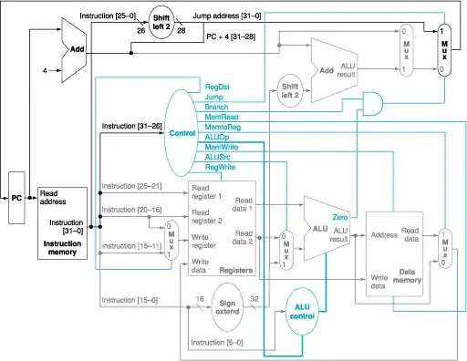
enter image description here

obe
  • 117
  • 5

4 Answers4

4

In the case of word-aligned reads, the upper address bits (A1 .. A19) are the same for both bytes. So the upper address bits don't change, and the whole word can be addressed in one read operation.

In the case of byte-aligned reads, the upper address bits must change, because there's a carry out of that least significant address bit. Because at least one upper address bit does change, the read needs to happen in two operations.

Work out, on paper, the transactions needed between the CPU and the memory to do an aligned word read, and a non-aligned word read. The issue should be clear at that point.

TimWescott
  • 44,867
  • 1
  • 41
  • 104
  • Do you mean that the address has to be changed on the address bus, and it's not enough to change it "locally" within the memory controller circuit? I'm not sure I understand what you mean by "there's a carry out of that least significant address bit"... – obe Aug 31 '19 at 17:14
  • The CPU is putting **physical voltages** onto its address pins. It can only put 19 unique voltages on those pins at a time, and the memory can only respond to those 19 voltages, which **address a word**. How can such an assembly address **two words at once**? – TimWescott Aug 31 '19 at 17:22
  • Yes, the address has to be changed on the address bus and the CPU has to wait for the second word to arrive. For an unaligned read, it reads two words, and throws half of each of them away. – pjc50 Aug 31 '19 at 17:26
  • @TimWescott I don't see why the CPU needs to address *two words* at once. It needs to address two bytes, but supply a different address to each memory bank. It can manipulate the address of the "even" memory bank using an adder, as I show in the circuit diagram (which does work in simulation...) – obe Aug 31 '19 at 18:28
  • @TimWescott you write "the memory can only respond to those 19 voltages". Why can the memory only respond to these voltages? Why is the manipulation I do in the circuit diagram with the adder wrong? – obe Aug 31 '19 at 18:40
  • There is one, 16-bit wide memory bank. There is no "each memory bank". There is just **one**. – TimWescott Aug 31 '19 at 18:41
  • "Why can the memory only respond to these voltages?" Please refer to a [data sheet of the 8086](https://www.archive.ece.cmu.edu/~ece740/f11/lib/exe/fetch.php?media=wiki:8086-datasheet.pdf). How many address pins do you see? How could you independently address two memory banks from those pins? – TimWescott Aug 31 '19 at 18:44
  • @TimWescott you wrote: 'there is no "each memory bank", there is just one'. According to this diagram: https://www.screencast.com/t/LsRkwJkl7G , from "Microprocessors and Microcontrollers" by Krishna Kant, there are "lower-order byte memory bank" and "High-order byte memory bank"... is it wrong? – obe Aug 31 '19 at 18:52
  • Yes! I did! That's because "each memory bank" implies more than one -- and there is just one. Why don't you read [the 8086 data sheet](https://www.archive.ece.cmu.edu/~ece740/f11/lib/exe/fetch.php?media=wiki:8086-datasheet.pdf)? – TimWescott Aug 31 '19 at 18:54
  • @TimWescott I apologize, I accidentally submitted that comment before I finished writing it. I edited it now, please see. I did read the 8086 data sheet, I understand that there is just one address bus with 20 address bits. So does the diagram I added in the question, but it can still get 16-bit of data in an unaligned read in a single clock cycle... – obe Aug 31 '19 at 18:56
  • Yes, but you just **doubled** the number of address lines. Where do you envision those to be placed? Inside the CPU? Your CPU and PCB need two address buses (See my update answer below). Inside the memory? Your memory needs an adder and a aligned/unaligned pin. and twice as much address line and address decoding. On the PCB? You need and adder and two memory banks each with a separate address decoder. Your idea is not impossible, just inefficient. – Oldfart Aug 31 '19 at 19:16
  • Ok, I thought to place it in the memory, with the adder, yes. So: (1) if the issue is inefficiency, essentially all the other answers here, claiming that it's not doable, are in fact wrong?, (2) in what way would it be considered inefficient? as I understand, if the added logic can be applied within the boundaries of a single clock cycle, wouldn't it offer the same performance with aligned reads, and better performance with unaligned reads? Or does "inefficient" refer to other costs? – obe Aug 31 '19 at 19:23
  • 1: It can't be done because the 8086 doesn't have an addressing mode that supports it. The 8086 isn't some imaginary thing that does what you want. It's a **chip** that comes pre-packaged and does what it does. 2: Adders are big and slow. If the logic is working at the limits of its clock speed, then there wouldn't be *time* to compute the second address, even if it's just +1. You could maybe marry a real 8086, running at 1980 speeds, to current logic running at 2019 speeds -- but the 8086 still doesn't have an addressing mode for that. – TimWescott Aug 31 '19 at 19:28
  • 1: Of course I understand that the 8086 cannot be "made" to work like that. What I mean by "can be done" is "it is a valid alternative implementation that would work". Since the designers of the 8086, who were likely smarter than me and for sure more knowledgeable, followed a different design which requires an extra clock cycle compared to my design, I'm trying to understand why my design is wrong or less favorable. – obe Aug 31 '19 at 19:33
  • 2: Ok, so from this I understand that the adder would be either too big to fit physically, or too slow to fit in a single clock cycle (I assume together with all other stuff that needs to happen during that cycle). Is that what you meant?, and (3) side question: does it take the 8086 ALU more than a single clock cycle to perform 16-bit addition? – obe Aug 31 '19 at 19:35
  • What I meant by the adder being big and slow is that if you have the resources for a 20-bit adder in your system, you may be able to get more speedup by applying those resources to something other than the scheme you've come up with. – TimWescott Aug 31 '19 at 19:37
  • I'm not sure how long the 8086 ALU takes to do a 16-bit addition, or whether it's pipelined. – TimWescott Aug 31 '19 at 19:38
  • @TimWescott thank you for the explanations! – obe Aug 31 '19 at 19:55
4

Nope!

The memory has only one address bus. Let me explain why that is relevant.

Lets assume a 64K 16-bit wide memory. The memory physical address bus is then A0..A15. But each of those addresses read/writes two bytes.

This is where a lot of people have problems: this memory address bus is NOT connected one-to-one to the CPU address bus. The CPU address lines are connected as:

  • CPU A0 => Not connected to memory*
  • CPU A1 => MEM A0
  • CPU A2 => MEM A1
  • ...
  • CPU A16 => MEM A15

This leads to the following diagram:
enter image description here

Now lets have a look at your unaligned address:
You want to read 16-bits from lets say address 3 & 4. But the location which the CPU sees as 3 and 4 are in memory locations 1 and 2. As you can see the only way to get to those is

  • first read memory location 1, read the byte and holds it.
  • Then read memory location 2 and pass both bytes to the CPU.

(On the way there they are re-ordered as you have shown in your MUX diagram above.)

Thus an unaligned address takes two memory accesses to read one 16-bit wide word.

-------------- Some more words:

Your scheme is not totally impossible.
To implement it you would need:

  • A CPU with two address buses. (Let's called them upper and lower)
  • Two separate 8-bit wide memories each using one of these address buses.

To do an aligned access the CPU would output the same address on both upper and lower address bus. To do an unaligned access the CPU would output address X on one bus and X+1 on the other.

So now you can do aligned an unaligned data access in one cycle, but you have just doubled the amount of address lines and the address bus routing on the PCB.

*Internally in the CPU the A0 address bit is used and is connected to a MUX. This mux is used among others for byte access and it 'moves' the byte from the dataline [15:8] to [7:0].

Oldfart
  • 14,212
  • 2
  • 15
  • 41
  • If I understand correctly, in your answer you portray the memory as an array of 16-bit cells. But as I understand, this is not the case with the 8086 (or with any other commercial computer, AFAIK). The underlying memory is always an array of 8-bit cells, each cell technically addressable individually... – obe Aug 31 '19 at 18:33
  • First, nope. Not even today is memory necessarily addressed in bytes (see the TMS320F2028 and other DSP chips for a current example, the IBM 360 for older examples). Second, nope. The [logical memory arrangement of the 8086](https://www.archive.ece.cmu.edu/~ece740/f11/lib/exe/fetch.php?media=wiki:8086-datasheet.pdf) is an array of 16 bit words. You can suppress *writes* on a byte-by-byte basis, but the *words* are always addressed 16 bits at a time. – TimWescott Aug 31 '19 at 18:48
  • That is exact why I wrote: "*"This is where a lot of people have problems"* The CPU address space is in bytes but most memories these days are 32 or even 64 bits wide. – Oldfart Aug 31 '19 at 18:53
  • Like I wrote in a comment for TimWescott's answer, the book "Microprocessors and Microcontrollers" explicitly states that the memory is split into two banks, each addressed at an 8-bit granularity ( https://www.screencast.com/t/LsRkwJkl7G ). Also, I don't understand why such a scheme would require two address buses (outside of the memory module itself). The "second" address would always be "first address" plus one. Why can't it be calculated with an adder inside the memory control module, independent of the CPU? (like in my diagram...) – obe Aug 31 '19 at 19:15
  • *"The "second" address would always be "first address" plus one."* That is where your error is because now you just made *aligned* access not possible. For aligned access you need X and X to each 8-bit bank, for unaligned access you need X and X+1 to each 8-bit bank. Your memory chip would need two address decoders, one for each bank. – Oldfart Aug 31 '19 at 19:20
  • Because, first, there is no "memory control module", or if there is it's just a few demultiplexers, and second, because the 8086 simply doesn't *do* non-aligned word memory accesses as anything other than two byte-wide accesses. – TimWescott Aug 31 '19 at 19:22
  • @Oldfart thank you for the explanations! – obe Aug 31 '19 at 19:56
1

You proposed idea would require a 20-bit adder in the address path, which is a critical path for determining RAM R/W access time. In the 8086 time frame, 20-bit adders were slow enough that the memory access time could be significantly impacted, thus slowing down all aligned reads, increasing costs and decreasing benchmark performance numbers (since aligned reads are far more common).

hotpaw2
  • 4,731
  • 4
  • 29
  • 44
  • But if it still falls within the boundaries of an 8086 clock cycle, why would it make a difference for aligned reads? – obe Aug 31 '19 at 16:57
  • @obe that's what hotpaw2 is saying: it *doesn't* fall in the "spare" time in that clock cycle. – Marcus Müller Aug 31 '19 at 17:06
  • I see... but how is that possible? Don't other lengthy operations complete within a clock cycle (like 16-bit addition or multiplication)? Is it the additional few bits that make this difference..? – obe Aug 31 '19 at 17:16
  • Look up 74LS83 worse case carry propagation delay. Multiply by 5 (for 20 bits) Compare to clock cycle time. – hotpaw2 Aug 31 '19 at 17:26
  • @hotpaw2 ok, I haven't checked the specs (yet) and intuitively it "feels" wrong (to me), but obviously if that's the case then it's a good explanation. I wonder why it didn't get votes, while the other answers did. I (still?) don't see how they answer my question and explain why my circuit diagram would not work in "real life"... – obe Aug 31 '19 at 18:37
0

When the 8086 sees a misalign that straddles a bus width boundary, it breaks the access up into multiple cycles. Unless you make your own 8086, that’s fixed in microcode and can’t be tricked into behaving differently.

What you’re proposing is a variation of a technique called a prefetch or read-ahead. It’s a valid approach, but only if the host can take advantage of it. Which the 8086 can’t.

In reality misaligns can be avoided by the compiler ensuring that critical variables and data structures are aligned in memory for efficiency.

hacktastical
  • 49,832
  • 2
  • 47
  • 138
  • I understand that the 8086 does it in two cycles... what is not clear to me is why it was designed this way. In other words: what is the problem or disadvantage of the design in my diagram... – obe Aug 31 '19 at 19:17
  • The prefetch will require a separate address bus. This is 20 more pins. Remember, the 8086 is in a 40-pin DIP so it is very constrained this way. – hacktastical Aug 31 '19 at 19:21