6

I'm switching a 12V 500mA resistive load (LED strip) with a IRF540 MOSFET and it's getting very hot when it's on and conducting.

CircuitLab Schematic qs4g4dfh3rr7

This confuses me as MOSFETs are supposed to have very low on-resistance and be great for power-switching applications. I'm driving the gate at 12V, and the data sheet says that the IRF540's RDS is 0.077Ω at a VGS of 10V, so at 500mA current it should be dissipating a tiny amount of energy:

P = I2 ⋅ R

P (W) = (0.5)2 (A) ⋅ 0.077 (Ω)

P (W) = 0.01925

... but what I see must be dramatically greater than that, because the TO-220 package gets too hot to touch comfortably after a minute or so. CircuitLab says ≈ 1.8W which seems more reasonable from the heating observed.

What's my beginner mistake?

Edit: If you're reading this and interested in driving LED strips, see also Design considerations for LED strip PWM dimming .

Craig Ringer
  • 253
  • 2
  • 11
  • FWIW, I would reduce the value of resistor RG_Pulldown to 10 kohms, or something close to that. The present 50 megohm resistance will cause a very long shutoff time for the NMOS transistor which might be bad for the NMOS. You want the NMOS to switch between ON and OFF as quickly as possible to minimize power dissipation in the NMOS. Also, why is resistor LED_Discharge needed? – Jim Fischer Jun 10 '19 at 06:22
  • @JimFischer R_Led_Discharge is only there to shut up CircuitLab, which otherwise insists that there is a significant voltage on the LED side even when the switch to the MOSFET gate is off. Thanks for the tip re the other resistor - I want to limit unnecessary power dissipation since it's a 12V circuit there, so if I go for something lower valued I might need a smarter method. Or maybe it's insignificant. – Craig Ringer Jun 11 '19 at 00:47
  • Follow-up: issues using a 555 as a driver (https://electronics.stackexchange.com/q/443950/146535) . – Craig Ringer Jun 17 '19 at 02:25

2 Answers2

12

The only mistake is using the NFET as a high side switch when it should be a low side switch with Vs=0V then with Vgs>=10V you pull down the load cathode and series R from the supply with the drain.

So transistors used as switches (FETs and BJT’s) are always inverting. Vgs is chosen from the specs or as a rule of thumb Vgs>2.5 x Vt(max) the threshold of conduction, also known as Vgs(th).

Tony Stewart EE75
  • 1
  • 3
  • 54
  • 182
  • Gah! So I don't need any fancy gate driver circuitry to boost the gate voltage above the supply. Thankyou. – Craig Ringer Jun 10 '19 at 05:16
  • I'll try to do a fixed up circuit example soon. Then some desoldering... – Craig Ringer Jun 10 '19 at 05:20
  • Yet in a half bridge using both NFETs, the low side does PWM and also with a cap provides a charge pump to driver IC’s to create the boost Vb above V+ to pull up the high side. – Tony Stewart EE75 Jun 10 '19 at 06:12
  • 4
    This must be what it feels like when I explain advanced postgres queries to people. *blink* *blink* – Craig Ringer Jun 10 '19 at 06:20
  • 2
    @CraigRinger, if your MOSFET is a power MOSFET that must switch lots of amps, then you should use a gate drive circuit/IC to ensure the MOSFET turns ON|OFF as fast as possible, in order to minimize the power that's dissipated by the transistor. Driving the gate with, say, a microcontroller's digital output pin does not source/sink enough "gate drive" current to the ensure the power MOSFET rapidly switches from cutoff mode (OFF) into its ohmic region (ON), and vice versa. – Jim Fischer Jun 10 '19 at 06:28
  • OK, gotcha. I gathered that from the docs I read recently. I'm only switching 500mA but it might be interesting anyway to minimise losses, I'd like to be able to use it with PWM so a fast low-loss on/off will be desirable even at 500mA. The "totem pole" gate drive design looks like something I could implement, if not necessary confidently understand and explain. – Craig Ringer Jun 10 '19 at 06:35
  • Impedance ratios are usually 1000:1 from gate driver to drain load as a rough rule of thumb with the RdsOn about 1% of load – Tony Stewart EE75 Jun 10 '19 at 06:38
  • Mind explaining "series from the supply with the drain"? Sorry... – Craig Ringer Jun 10 '19 at 06:55
  • 1
    bad keybd. Series (R). I just meant the load is on high side to supply switch is on low side. – Tony Stewart EE75 Jun 10 '19 at 13:46
  • Thanks. Added corrected circuit diagram here: https://www.circuitlab.com/circuit/z9k24f7nd5gj/mosfet-led-strip-switching-fixed/ . No dedicated gate drive, no capacitors, etc, so probably unsuitable for fast switching, but at least it switches without cooking the MOSFET. Hopefully. – Craig Ringer Jun 11 '19 at 07:29
7

TL;DR: I was driving my MOSFET gate at the supply voltage I was switching/ so I didn't maintain a high enough VGS. I'd failed to consider that Vs is not 0V once the MOSFET is on.

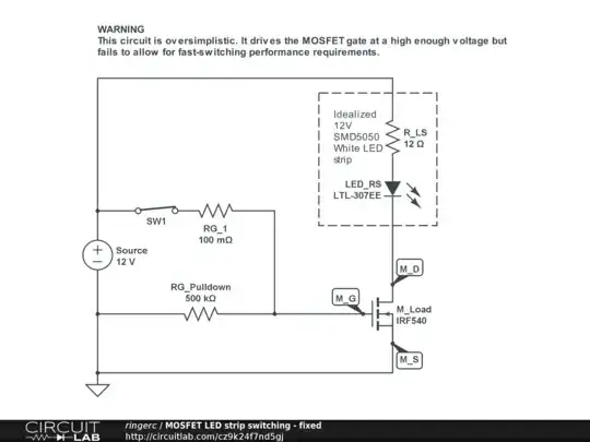
Per the accepted answer the simplest solution to that is putting the MOSFET on the low (ground) side so that VS ~= 0, making VGS easy to keep high. See corrected (but warning, still way too simplistic) circuit:

CircuitLab Schematic z9k24f7nd5gj

See tutorial article "MOSFET as a switch" and many others.

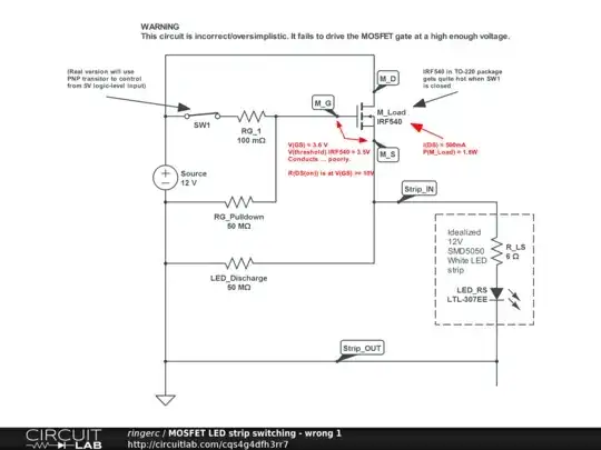
The immediate problem with the circuit in the question

The critical point is that the MOSFET's low resistance state Rds(on) is achieved when VGS is well above the gate threshold ... but not when VS is at 0V ground reference level. What matters is VGS when VS is at VD (with some handwaving for voltage drop across the MOSFET).

So if you are switching your supply voltage, your gate drive must be well above your supply voltage. That way your gate-to-output voltage is maintained and the MOSFET is kept in its low-resistance fully-on state.

The total charge required to switch the MOSFET from off to on is quite small and the gate current once it's fully on is tiny. So a variety of circuits can be used to boost VGS by increasing gate drive voltage above supply level. They don't waste much power because there's negligible current through them most of the time.

But you can't just drive the gate at the same voltage as the MOSFET's drain. It'll conduct because the VDS(drop) - the voltage drop across the drain-to-source path - maintains a nonzero VGS above the threshold voltage. But it won't get to the "on" VGS voltage needed to maintain efficient, low-resistance conduction.

I plan to add a schematic with a boosting gate driver of some kind soon. If anyone else has one, please share.

This great if in-depth article on MOSFET principles and applications shows some MOSFET gate-drive circuits.

If you're here you might find this article explaining MOSFET parameters useful too.

Making it work with a 3.3V input and PWM

A 3.3V input doesn't turn the gate on well enough to reliably reach RDS(on) on this MOSFET. Others are available that work at "logic level" gate signals. But you still don't want to drive them over a long wire from the microcontroller or PWM source.

This circuit will drive the MOSFET from a 3.3V input by using a low-side-switching NPN transistor for active pull-down and a resistor for passive pull-up. It's inverting, meaning the MOSFET is on when the 3.3V signal off and vice versa.

CircuitLab Schematic g6r79m5u4shq

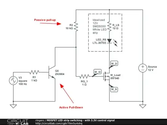
But .... relying on a resistor for pullup means it wastes power when on, as it produces a constant current. It also limits PWM speeds because the gate takes time to charge from the pull-up resistor and that means the MOSFET takes too long to turn on, wasting power (and producing heat) during its extended turn-on phase.

Really we want to actively drive the gate both down and up.

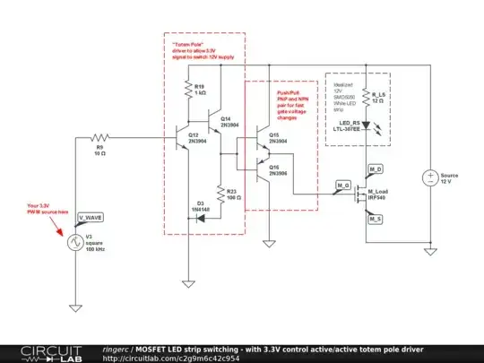
An active/active driver with discrete components

Here's my best effort so far, using a "totem pole" to switch 12V with a 3.3V input then a push/pull to drive the gate actively. It seems excessively complex though.

CircuitLab Schematic 2g9m6c42c954

Craig Ringer
  • 253
  • 2
  • 11
  • 2
    Be careful thinking that the total charge needed to turn a MOSFET on and off is quite small. For some MOSFETs the effective GATE capacitance can be quite large and in order to switch the device on and off quickly the gate driver may be required to source or sink many amps of current during the transition period. – Michael Karas Jun 10 '19 at 08:48
  • 1
    While having a voltage available for the gate which is boosted well above your supply voltage (the voltage you want to switch), is certainly an option, it's usually *significantly* less expensive to use your N-channel enhancement mode MOSFET (equivalent operation to many/most Power MOSFETs, such as the IRF540) to switch the low voltage side (i.e. ground) for your load. For your circuit, this is mostly swapping the position of your LED strip and the IRF540. [Note: Your RG_Pulldown resistor is almost certainly significantly too large.] – Makyen Jun 10 '19 at 22:50
  • Can somebody explain how and for what purpose D3 is being used here? Actually, a full discussion of the design would be awesome ... it's far more complex than the ones above it, but no description of what's really going on :-( – Sixtyfive Apr 16 '21 at 23:50